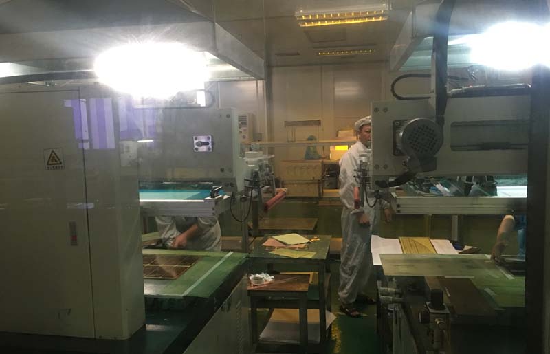
Rigid flex PCB Graphics transfer
Graphics transfer in high-density, thin lines of printed circuit board occupies a very important position, especially, for the flexible circuit.
Because the flexible monolithic is thin and soft, to the surface treatment and other operations bring great difficulties, and copper foil surface cleanliness and roughness of a direct impact on the adhesion of dry film corrosion resistance and thin lines of production.
As the mechanical rub plate on the equipment requirements are high, and the pressure may cause undesirable substrate deformation, roll, size expansion and contraction, the operation is not easy to control, so we can choose to use electrolytic cleaning method.
This method can ensure the surface cleanliness, while the use of micro-etching method to ensure the roughness of the copper surface is conducive to 0.1mm ~ 0.15mm line width / spacing line graphics production.
Acid etching In addition to attention to control the etching rate to ensure that the design requirements of the line width, spacing, but also to prevent the curling of a single piece, wrinkles, preferably with auxiliary guide plate and turn off the equipment ventilation system.
Rigid flex PCB lamination
The dimensional stability of the flexible substrate is poor because the polyimide material has a strong moisture absorption property,Or in different temperature and humidity environment,
serious deformation shrinkage, resulting in multilayer laminating difficult position.
In order to overcome this difficulty, the following measures can be used: the design to consider the location of the spot and the design of the punching spot in order to ensure punching holes in the hole or rivet holes when the accuracy, and will not cause the stack The deviation between the layers of graphics resulting in scrapped.
OPE punched hole after positioning, can eliminate the wet process of material deformation caused by the error.
After lamination, the holes were drilled with X-ray to determine the offset and make the drilling more accurate. According to the material properties and environmental characteristics of the polyimide, the outer film was drawn with reference to the borehole offset to improve the coincidence degree between the outer film and the drilling plate. In this way, we can meet the interlayer alignment to ensure 0.1mm ~ 0.15mm ring width requirements, to ensure the accuracy of the outer graphics transfer.
Browse our website for more information about rigid flex pcb.
By Andwin TechTeam