Chemical copper is a very important step in the process of metallization of printed circuit boards. The purpose is to form an extremely thin conductive copper layer on the walls and copper surfaces for the subsequent plating. And hole wall coating hole is printed circuit board hole one of the common defects in metal, but also easy to cause printed circuit board batch scrapped one of the items, so to solve the printed circuit board coating hole problem is the PCB manufacturers focus on control , But because of the causes of its defects are varied, only the accuracy of the characteristics of its defect can effectively find out the solution to the solution.
1, PTH hole hole caused by the hole coating
PTH hole hole caused by the hole is mainly point-like or circular cavity, the specific reasons are as follows:
Talking about the Cause and Countermeasure of the Wall Hole of the Circuit Board – “Journal of the China Society for Scientific andTechnical Information”
(1) PHT copper content, sodium hydroxide and formaldehyde concentration
The concentration of the copper cylinder solution is the first consideration. In general, the copper content, sodium hydroxide and formaldehyde concentration is proportional, when any of the content below 10% of the standard value will destroy the balance of chemical reactions, resulting in poor chemical copper deposition, Of the empty. So give priority to adjust the copper cylinder of the syrup parameters.
(2) the temperature of the bath
The temperature of the bath also has an important effect on the activity of the solution. In the solution will generally have the temperature requirements, some of which are to be strictly controlled. So the temperature of the bath should also be concerned about the temperature.
(3) control of the activator
The low dibasic tin ions can cause the decomposition of colloidal palladium, which affects the adsorption of palladium, but as long as the activation of the timing of the addition of added,
will not cause a big problem. Activated liquid control is the focus of the air can not be stirred, the oxygen in the air will oxidize the divalent tin ions, but also can not have water into,
will cause the hydrolysis of SnCl2.
(4) the temperature of the cleaning
Cleaning the temperature is often overlooked, the best cleaning temperature is above 20 ℃, if less than 15 ℃ will affect the cleaning effect. In the winter, the water temperature will change very low, especially in the north. As the water temperature is low, the temperature of the board after the cleaning will become very low, the temperature of the board after entering the copper cylinder can not immediately rise, because of the golden time to miss the deposition of copper deposition effect. So the lower the ambient temperature, but also pay attention to the temperature of cleaning water.
(5) the use of the hole agent temperature, concentration and time
The temperature of the liquid has a more stringent requirements, too high temperature will cause the decomposition of the pore agent, so that the concentration of the hole agent becomes low, affecting the effect of the whole hole, its obvious feature is in the hole in the glass fiber cloth Appear dotted voids. Only the temperature of the liquid, the concentration and time with the proper, in order to get a good effect of the whole hole, while saving costs. The concentration of copper ions accumulated in the liquid must also be strictly controlled.
(6) the use of reducing agent temperature, concentration and time
The effect of the reduction is to remove residual potassium permanganate and potassium permanganate after drilling, and the loss of control of the relevant parameters of the drug will affect its effect. The obvious feature is the occurrence of dot-like voids at the resin in the pores.
(7) Oscillator and swing
Oscillator and swing out of control will cause a circular cavity, which is mainly due to the hole in the bubble can not be ruled out to high thickness ratio of the orifice plate is most obvious. Its obvious feature is the hole of the hole symmetry, and the hole part of the copper copper normal, graphic plating (secondary copper) wrapped in the whole board coating (a copper).
2, the hole caused by the transfer of holes in the hole
Graphic transfer caused by the hole wall coating hole is mainly the hole ring and hole in the hole in the hole, the specific reasons are as follows:
(1) pre-treatment brush plate
The pressure of the brush plate is too large, the whole copper and PTH hole at the copper layer was brushed off, so that the back of the graphics plating can not be coated with copper, resulting in holes annular hole. The obvious feature is that the copper layer of the orifice is gradually thinned, and the graphic plating layer wraps the whole board coating. So by doing wear marks test, control brush plate pressure.
(2) hole residual glue
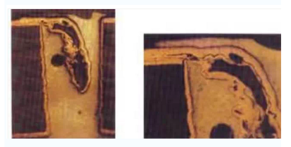
In the graphics transfer process on the control of the process parameters is very important, because the pretreatment of poor drying, foil temperature, the pressure will cause the edge of the mouth of the residual parts of the hole caused by the hole of the hole. The obvious feature is that the thickness of the copper layer in the hole is normal, the annular orifice at the single or double-sided orifice is extended to the pad, and the edges of the fault are clearly etched. The graphic plating does not wrap the entire board (see image 3).
(3) pretreatment micro etch
Pretreatment of micro-etching to be strictly controlled, in particular, to control the number of dry film rework. Mainly in the middle of the hole due to the problem of plating uniformity of the thickness of the coating is too thin, too much rework will cause the whole hole within the copper layer thinning, and eventually produce the middle of the hole ring copper. The obvious feature is that the entire board of the hole is gradually thinned, and the pattern plating layer wraps the whole board coating (see Fig. 4).
3, graphics plating caused by hole wall coating hole
(1) Graphic plating micro etch
Graphic electroplating of the micro-eclipse should also be strictly controlled, the resulting defects and dry film pretreatment micro-corrosion is basically the same. Serious wall when the wall will be a large area without copper, the board on the board thickness was thin. Therefore, to measure the rate of micro-etching, it is best to optimize the process parameters through DOE experiments.
(2) tin (lead tin) poor dispersion
Due to poor solution performance or rocking and other factors so that the thickness of tin plating coating in the back of the film and alkaline etching when the hole in the middle of the tin layer and copper layer erosion, resulting in annular cavity. The obvious feature is that the thickness of the copper layer in the hole is normal and the edges of the fault are clearly traces of the etched, and the patterned plating layer is not wrapped around the board (see Figure 5). In this case, you can add some tin plating agent before tinning, can increase the wettability of the board, while increasing the amplitude of the swing.
4 Conclusion
There are many factors that cause the voids of the coating. The most common is PTH coating voids, which can effectively reduce the void formation of PTH coating by controlling the relevant process parameters of the syrup. But other factors can not be ignored, only through careful observation, to understand the causes of the cavity and the characteristics of defects in order to timely and effective solution to the problem, maintaining product quality.