PCB desgin and PCB layout knowledge tips
The design requirements include electrical and institutional parts.
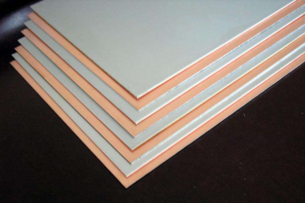
This material problem is usually important when designing very high speed PCB boards (frequencies greater than GHz).
For example, the commonly used FR-4 material, dielectric loss at several GHz frequencies, can have a significant effect on signal attenuation and may not be used. In the case of electrical, it is important to note whether the dielectric constant and the dielectric loss are combined at the designed frequency.
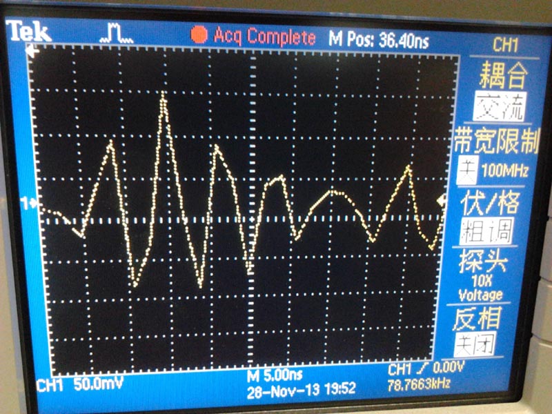
the high-frequency signal electromagnetic field, that is, the so-called crosstalk .
Can be used to pull the high-speed signal and the distance between the analog signal,
or ground guard / shunt traces next to the analog signal.
Also pay attention to the digital ground to the analog ground noise interference.
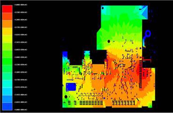
The factors that affect the impedance matching are the architecture of the signal source and the output impedance, the characteristic impedance of the trace, the characteristics of the load side, the topology architecture, and so on.
The solution is * termination and alignment of the topology
One is the length of the two lines to the same length,
The other is the distance between the two lines (this distance determined by the differential impedance) to remain the same,
That is, to keep parallel.There are two parallel ways, one for the two lines walking in the same line layer (side-by-side),
one for the two lines in the upper and lower adjacent two layers (over-under).
Generally in front of the side-by-side to achieve more ways.
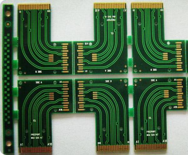
So for only one output of the clock signal is unable to use the differential wiring.