Super complete PCB Failure Analysis Technology
PCB as a carrier of various components and circuit signal transmission hub has become the most important electronic information products and the key part of its quality and reliability of the quality of the machine determines the quality and reliability.
With the miniaturization of electronic information products and lead-free halogen-free environmental requirements, PCB to high-density high-Tg and environmentally friendly direction. However, due to cost and technical reasons, PCB in the production and application process there have been a lot of failure problems, and thus triggered a lot of quality disputes. In order to find out the reasons for the failure in order to find a solution to the problem and to clarify the responsibility, the failure of the case must be a failure analysis.
The basic procedure for failure analysis
To obtain the exact cause or mechanism of PCB failure or failure, you must abide by the basic principles and analyze the process, otherwise it may miss valuable invalidation information, resulting in analysis can not continue or may get the wrong conclusion. The general basic process is to first determine the failure and failure modes, ie, failure location or fault location, through information collection, functional testing, electrical performance testing, and simple visual inspection based on the failure phenomenon.
For a simple PCB or PCBA, the failure of the site is easy to determine, but for more complex BGA or MCM package devices or substrates, defects difficult to observe through the microscope, sometimes difficult to determine, this time need to use other means to determine.
The mechanism of failure or defect, such as Weld, Pollution, Mechanical Damage, Moisture Stress, Dielectric Corrosion, Fatigue Damage, CAF or Ion Migration, is analyzed by various physical and chemical means, Stress overload and so on.
Then, based on the analysis of failure reasons, that is based on the failure mechanism and process analysis, find the cause of the failure mechanism of the reasons, if necessary, test validation, generally as far as possible possible test validation, through experimental verification can find the exact cause of failure.
This provides a targeted basis for the next step of improvement. Finally, according to the analysis process obtained by the test data, facts and conclusions, the preparation of failure analysis report, the report of the facts clear, logical reasoning rigorous, structured, avoid imagination.
During the analysis process, the use of analytical methods should be from simple to complex, from outside to inside, never destroying the sample and then using the basic principles of destruction. Only in this way can we avoid the loss of key information, to avoid the introduction of new human failure mechanism.
It is like a traffic accident, if the accident side of the destruction or escape from the scene, in the clever police is also very difficult to make an accurate responsibility that time, traffic regulations generally require people to flee the scene or destroy the scene to assume full responsibility.
PCB or PCBA failure analysis is the same, if the use of electric soldering iron on the failure of the solder joint repair or large scissors to cut the PCB, then the reanalysis can not start, the failure of the scene has been destroyed. Especially in the case of less failure samples, once the damage or damage to the scene of the failure of the scene, the real failure can not be obtained.
Failure analysis technology
Optical microscope
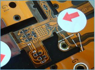
Optical microscope is mainly used for the appearance of PCB inspection, to find the site of failure and related physical evidence, the initial failure to determine the PCB model. The main inspection of the PCB inspection of the pollution, corrosion, explosion board position, circuit wiring and failure of the regularity, such as batch or individual, is not always concentrated in a region and so on.
X-ray (X-ray)
For some of the parts can not be detected by the appearance of the PCB and the hole through the internal and other internal defects, had to use X-ray fluoroscopy system to check.
X-ray fluoroscopy system is the use of different material thickness or different material density X-ray moisture absorption or transmittance of different principles to imaging. The technology is more used to check the defects inside the PCBA solder joint, through-hole internal defects and high-density packaging BGA or CSP device defective solder joint positioning.
Slice analysis
Slicing analysis is through the sampling, mosaic, slicing, grinding, corrosion, observation and a series of means and steps to obtain PCB cross-sectional structure of the process. Through the analysis of slices can be reflected PCB (through hole, coating, etc.) the quality of the microstructure of the rich information for the next step to improve the quality of a good basis. But the method is destructive, once the slices, the sample will inevitably be destroyed.
Scanning Acoustic Microscope
Currently used for electronic packaging or assembly analysis is mainly C-mode ultrasonic scanning acoustic microscope, which is the use of high-frequency ultrasound in the material discontinuous interface reflection of the amplitude and phase and polarity changes to imaging, the scan is along the Z-axis scan X-Y plane information.
Therefore, scanning acoustic microscopes can be used to detect components, materials, and PCB and PCBA internal defects, including cracks, layers, inclusions and voids. If the frequency of the scanning acoustics is sufficient, the internal defects of the solder joint can be detected directly.
A typical scanning acoustic image is a red warning color that indicates the presence of defects due to the large number of plastic encapsulated components used in the SMT process, from lead to lead-free process, a large number of wet return sensitive problems arise, That is, moisture-absorbing plastic device will be higher in the lead-free process temperature reflux when the internal or substrate layered cracking phenomenon in the lead-free process of high temperature ordinary PCB will often appear burst board phenomenon.
At this point, scanning the acoustic microscope to highlight its multi-layer high-density PCB nondestructive testing of the special advantages. And the general obvious burst board is only through the visual appearance can be detected.
Microscopic infrared analysis
Microscopic infrared analysis is the infrared spectroscopy and microscopy combined with the analysis method, which uses different materials (mainly organic matter) on the infrared absorption of different principles of the composition of the material composition, combined with the microscope can be visible and infrared light with the same Light path, as long as the visible field of view, you can find to analyze trace amounts of organic pollutants.
If there is no combination of microscopes, usually infrared spectroscopy can only analyze the sample volume of more samples. The electronic process in many cases is the trace of pollution can lead to PCB pad or lead pin poor solderability, it is conceivable that there is no microscope supporting the infrared spectrum is difficult to solve the process problem. The main purpose of micro-infrared analysis is to analyze the surface of the weld or solder surface of organic pollutants, analysis of corrosion or poor solderability reasons.
Scanning Electron Microscopy (SEM)
Scanning electron microscopy (SEM) is one of the most useful large-scale electron microscopic imaging systems for failure analysis. Most commonly used for morphological observation. The current scanning electron microscopy has been very powerful and any fine structure or surface features can be amplified To hundreds of thousands of times to observe and analyze.
In the PCB or solder joint failure analysis, SEM is mainly used for the failure mechanism of the analysis, in particular, is used to observe the surface structure of the pad surface, solder alloy microstructure, measuring intermetallic, solderable coating Analysis and do tin whisker analysis and so on.
Unlike optical microscopes, scanning electron microscopy is made of electronic images, so only black and white, and scanning electron microscopy specimens require conductivity, non-conductor and some semiconductors need to spray or carbon treatment, or charge on the sample surface Sample observation. In addition, the scanning electron microscope image depth is far greater than the optical microscope, is for the metallographic structure, micro-fracture and tin whisker and other uneven samples of the important analytical methods.
Thermal analysis
Differential Scanning Calorimetry (DSC)
Differential Scanning Calorimation (Differential Scanning Calorim- etry) is in the program temperature control, the input to the material and the reference material between the power difference and temperature (or time) a way. Is to study the relationship between heat and temperature changes in the analysis method, according to this change in the relationship between the material can be studied the physical and chemical and thermodynamic properties.
DSC is widely used, but in the PCB analysis is mainly used to measure the PCB used in a variety of polymer materials, curing degree, glass transition temperature, these two parameters determine the PCB in the follow-up process reliability.
Thermomechanical analyzer (TMA)
Thermal Mechanical Analysis Used to measure the deformation properties of solids, liquids and gels under thermal or mechanical forces at programmed temperature control. Is the method of studying the relationship between heat and mechanical properties. According to the relationship between deformation and temperature (or time), the physical and chemical and thermodynamic properties of the materials can be studied and analyzed.
TMA is widely used in the PCB analysis is mainly used for PCB the most critical two parameters: measuring the linear expansion coefficient and glass transition temperature. PCBs with too large expansion coefficients often cause fracture of the metalized pores after welding assembly.
Thermogravimetric analyzer (TGA)
Thermogravimetry (Thermogravimetry Analysis) is in the program temperature control, measuring the quality of the material with the temperature (or time) a relationship between the changes. TGA through sophisticated electronic balance can monitor the material in the program-controlled temperature changes in the process of subtle changes in quality.
According to the material quality with temperature (or time) changes in the relationship between the material can be studied the physical and chemical and thermodynamic properties. In the PCB analysis, mainly used to measure the thermal stability of PCB materials or thermal decomposition temperature, if the substrate thermal decomposition temperature is too low, PCB in the welding process will occur when the high temperature blasting or stratification failure phenomenon.