Printed circuit boards are the most important part of electronic equipment.
With the popularity of electronic technology and the development of integrated circuit technology,
a variety of electromagnetic interference problems have emerged,
due to electromagnetic interference caused by economic losses are also increasing.
Therefore, electromagnetic compatibility is more and more important.
This paper aims to analyze the causes of electromagnetic interference in the PCB, and to explore its approach. In the case of
Electromagnetic interference in PCB
PCB interference is divided into two kinds.
One from the inside of the PCB, it is mainly due to the parasitic coupling between the adjacent circuits and the internal components of the field coupling,
the signal along the transmission path crosstalk. Such as capacitors on the PCB,
especially those used at high frequencies.
We can think of it as an LCR circuit, because the capacitor actually work in the circuit,
the general will produce equivalent inductance and impedance,
capacitance has a self-resonant frequency, at the self-resonant frequency,
the capacitor presents capacitive. At higher than the self-resonant frequency,
the capacitance is inductive and the impedance increases as the frequency increases.
In the case of Another kind of electromagnetic interference from the outside of the PCB,
it is divided into two kinds of radiation interference and sensitive elements.
Radiation mainly comes from the harmonics of the clock and other periodic signals,
as well as some electronic devices or instruments that generate secondary harmonics due to voltage and power transitions. In the case of
To avoid PCB electromagnetic interference, mainly from the following points:
1, reasonable design schematics
In the design of a circuit board, the first thing to do is the schematic design.
Design schematics generally use Altium Designer software to operate, the device can be used in the schematic library screening, if the schematic library does not have to select the device, you can draw. After drawing a good schematic, you need to perform automatic detection to check for obvious errors during the drawing process. In the case of
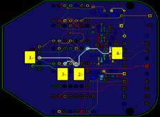
After the drawing is completed, the printed circuit board can be designed.
The results of automatic routing is always unsatisfactory, the need for manual layout and wiring. In the design of printed circuit boards, electromagnetic compatibility issues become an important technical requirements to consider. Reasonable layout of printed circuit boards in the layout of components and lines, can effectively reduce the electromagnetic interference problem. In the case of
2, choose its equivalent inductance and resistance of the relatively small capacitance
Crosstalk problems should also be taken seriously, crosstalk is the energy from one line coupled to another line. By Faraday’s electromagnetic induction phenomenon,
when a wire through the current, the wire will produce a magnetic field around. The magnetic field interaction of different wires will produce crosstalk. Mutual mutual inductance is one of the mechanisms that produce crosstalk,
and its size is proportional to the current in the wire. In the case of
3, the cycle signal is limited to a small area as small as possible
Mutuality is another mechanism that produces crosstalk, which is generated by the coupling of two electrodes through the electric field. The solution is to limit the periodic signal in a small area and block the coupling with the outside parasitic pathways, if necessary, can use the filter to filter; external sensitive mainly radio frequency interference and electrostatic discharge, to solve this problem You can use shield, good grounding and filtering methods. In the case of
4, the design of printed circuit board anti-jamming method
1) PCB board material selection. Printed circuit boards have single,
double and multi-layer board points. The most commonly used epoxy glass cloth as a substrate,
this material has the following advantages:
good expansion, is conducive to reducing the loop area,
reduce the differential mode interference,
low water absorption, heat resistance, chemical resistance,
impact Good performance. In the case of
2) PCB wiring.
Wiring to follow the minimum principle of flux, the minimum flux principle refers to the transmission line and the return path of the magnetic field lines offset each other to achieve the electricity flux cancellation.
Single-sided floor-free plane, the alignment point is to reduce the power circuit and signal loop circuit area. Use a ground protection trace.
Pull out the ground wire close to the power line or signal line together to reduce the loop area.
High-speed signal traces should be straight or obtuse,
should not appear acute and right angle. In the case of
3) PCB layout. In general, PCB design software has automatic layout function, but this feature does not meet the needs of the actual work,
so designers need to familiar with the rules of the layout.
Layout should be part of the digital circuit and analog circuit part of the separation, leaving a part of the middle of the space separated.
The layout should be based on the rate of high, medium and low speed,
I / O circuit partition, in order to reduce the high-speed circuit to other parts of the interference.
In the case of in conclusion
Printed circuit board design is a complex process,
the design needs to consider a lot of factors,
a little attention will be on the performance of the circuit board have a great impact.
In the design process, if not fully take into account the electromagnetic compatibility issues,
then the design of the circuit board is likely to not be put into use.
So the design should be fully taken into account the alignment, layout, grounding, shielding and other issues, to prevent crosstalk between the signal.