PCB guide hole distinction
The circuit board is made up of a layer of copper foil circuits, and the communication between the different circuit layers depends on the vias. This is because today’s circuit boards are manufactured using drill holes to connect to different circuits. The purpose of the layer, the connection is to conduct electricity, so it is called the via hole. In order to conduct electricity, a conductive material (usually copper) must be electroplated on the surface of the hole, so that the electron can be in different copper. The foil layers move between them because the surface of the original drilled hole is only electrically non-conductive.
Generally, there are three kinds of PCB vias (Via) that we often see, which are described as follows:
Through Hole: Plating Through Hole Abbreviation PTH
This is the most common type of via hole. You just need to pick up the PCB and look at the light. You can see that the light hole is a “through hole.” This is also the simplest kind of hole, because it is only necessary to use the drill bit or laser light to drill the board directly, and the cost is relatively cheap. Although the through hole is cheap, sometimes it will use more PCB space. For example, we have a six-story house. I bought it on the third and fourth floors. I want to design a staircase inside, only between the third and fourth floors. For me, the space on the fourth floor. Invisibly, it was used by the original first floor to connect to the stairs on the sixth floor.
Blind hole: Blind Via Hole (BVH)
The outermost circuit of the PCB is connected to the adjacent inner layer by a plated hole, and since it is not visible, it is called a “blind hole”. In order to increase the space utilization of the PCB circuit layer, a “blind hole” process has emerged. This method of production requires special attention to the depth of the drill hole (Z-axis). It is just right to drill the hole in the individual circuit layers before the circuit layer that needs to be connected, and finally glue it together, but it requires precise positioning. And alignment device. As an example of buying a building above, a six-story house is only connected to the first floor and the second floor, or the stairs connecting from the fifth floor to the sixth floor are called blind holes.
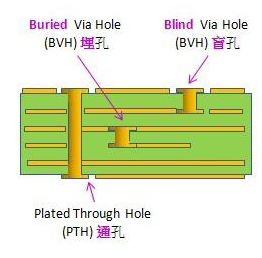
Buried hole: Buried Via Hole (BVH)
The connection of any circuit layer inside the PCB is not conducted to the outer layer. This process can not be achieved by means of bonding after drilling. It is necessary to perform drilling at the time of individual circuit layers. After partially bonding the inner layer, it must be electroplated first, and finally it can be fully bonded, compared with the original “through hole”. The “blind hole” takes more time, so the price is also the most expensive. This process is typically only used on high-density (HDI) boards to increase the usable space of other circuit layers. As an example of buying a building above, a six-story house has only a staircase connecting the third floor and the fourth floor, which is called a buried hole.
Grace Zheng
Email: sales06@andwinpcb.com
Skype: andwinpcb