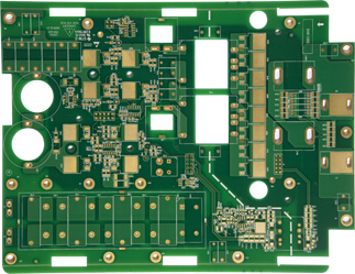
PCB layout and surface treatment process
PCB Chinese name is printed circuit board, also known as printed circuit board, printed circuit board, is an important electronic component, is the support of electronic components, is the provider of electrical connections of electronic components. Because it is made by electronic printing, it is called a “printing” circuit board. As PCB size requirements become smaller and smaller, device density requirements become higher and higher, and PCB design becomes more and more difficult. How to achieve high PCB layout and shorten design time, here to talk about the design skills of PCB planning, layout and wiring.
1 Determine the number of layers of the PCB
Board size and number of wiring layers need to be determined early in the design process. The number of wiring layers and the STack-up method directly affect the wiring and impedance of the printed wiring. The size of the board helps determine the stacking and line width to achieve the desired design. At present, the cost difference between the multi-layer boards is very small, and it is better to use more circuit layers and evenly distribute the copper at the beginning of the design.
2 Design rules and restrictions
To successfully complete the routing task, the routing tool needs to work under the correct rules and constraints. To classify all special required signal lines, each signal class should have priority. The higher the priority, the stricter the rules. The rules relate to the width of the trace, the maximum number of vias, the parallelism, the interaction between the signal lines, and the limitations of the layers. These rules have a large impact on the performance of the routing tool.
3 component layout
In the optimal assembly process, the manufacturability design (DFM) rules impose restrictions on the component layout. If the assembly department allows the components to move, the circuit can be properly optimized for easier automatic routing. The defined rules and constraints affect the layout design. The automatic routing tool only considers one signal at a time. By setting the wiring constraints and setting the layers of the signal lines, the routing tool can be routed as the designer envisions.
For example, for the layout of the power cord:
1 In the PCB layout, the power supply decoupling circuit should be designed near the relevant circuits, and should not be placed in the power supply. Otherwise, the bypass effect will be affected, and the ripple current will flow on the power line and the ground line, causing nuisance;
2 For the power supply inside the circuit, the power supply from the last stage should be taken, and the power supply filter capacitor of this part should be arranged near the last stage;
3 For some major current channels, such as disconnecting or measuring current during commissioning and testing, current gaps should be placed on the printed conductors during layout.
In addition, it should be noted that the regulated power supply is arranged on a separate printed board as much as possible. When the power supply and the circuit are used together with the printed circuit board, in the layout, it should be avoided that the regulated power supply is mixed with the circuit components or the power supply and the circuit are used together. Because this kind of wiring is not only easy to cause interference, but also can not break the load during maintenance, only a part of the printed wiring can be cut at that time, thereby damaging the printed board.
Although at present, the changes in the surface treatment process of PCBs are not very large, it seems to be a relatively distant matter, but it should be noted that long-term slow changes will lead to huge changes. As the environmental protection calls are getting higher and higher, the surface treatment process of PCBs will definitely change dramatically in the future.
The most basic purpose of surface treatment is to ensure good solderability or electrical properties. Since copper in nature tends to exist in the form of oxides in the air, it is unlikely to remain as raw copper for a long time, so other treatments of copper are required. Although in the subsequent assembly, a strong flux can be used to remove most of the copper oxide, the strong flux itself is not easily removed, so the industry generally does not use a strong flux.
There are many PCB surface treatment processes, and the common ones are hot air leveling, organic coating, electroless nickel/immersion gold, immersion silver and immersion tin, which will be introduced one by one.
1, hot air leveling (spray tin)
Hot air leveling, also known as hot air solder leveling (commonly known as spray tin), is a process of applying molten tin (lead) solder on the surface of the PCB and flattening (blown) with heated compressed air to form a layer that is resistant to copper oxidation. It also provides a good solderability coating. When the hot air is leveled, the solder and copper form a copper-tin intermetallic compound at the junction. The PCB is sunk in the molten solder during hot air leveling; the air knife blows the liquid solder before the solder solidifies; the air knife minimizes the meniscus of the solder on the copper surface and prevents solder bridging.,
2,Organic solderability protector (OSP)
OSP is a process that meets the requirements of the RoHS Directive for printed circuit board (PCB) copper foil surface treatment. OSP is the abbreviation of Organic Solderability PreservaTIves. Chinese translation is organic solder mask, also known as copper protector, also known as Preflux in English. Simply put, OSP chemically grows an organic film on a clean bare copper surface.
This film has anti-oxidation, thermal shock resistance and moisture resistance. It is used to protect the copper surface from rust (oxidation or vulcanization) in the normal environment. However, in the subsequent high temperature of welding, the protective film must be very It is easily removed by the flux, so that the exposed clean copper surface can be immediately combined with the molten solder into a firm solder joint in a very short time.
3, full plate nickel-plated gold
Nickel plated gold is plated with a layer of nickel on the surface conductor of the PCB and then plated with a layer of gold. The nickel plating is mainly to prevent the diffusion between gold and copper. There are two types of electroplated nickel gold: gold-plated gold (pure gold, the gold surface does not look bright) and hard gold (the surface is smooth and hard, wear-resistant, contains other elements such as cobalt, and the gold surface looks brighter). Soft gold is mainly used for gold wire bonding in chip packaging; hard gold is mainly used for electrical interconnection in non-welded parts.
4, Shen Jin
Shen Jin is a thick, electrically good nickel-gold alloy wrapped on the copper surface, which can protect the PCB for a long time; it also has environmental tolerance not available in other surface treatment processes. In addition, immersion gold can also prevent the dissolution of copper, which will benefit lead-free assembly.
5, Shen Xi
Since all current solders are based on tin, the tin layer can be matched to any type of solder. The immersion tin process can form a flat copper-tin intermetallic compound. This property makes the immersion tin have the same good solderability as the hot air leveling without the hot air leveling headache. The slab can not be stored for too long. The assembly must be carried out according to the order of the tin.
6, Shen Yin
The silver process is between organic coating and electroless nickel/immersion gold. The process is relatively simple and fast. Even if exposed to heat, humidity and pollution, silver can maintain good solderability, but it will lose its luster. . Silver does not have the good physical strength of electroless nickel/immersion gold because there is no nickel under the silver layer.
7,Chemical nickel palladium gold
Compared with immersion gold, chemical nickel-palladium gold has an additional layer of palladium between nickel and gold. Palladium can prevent corrosion caused by displacement reaction and is fully prepared for immersion gold. Gold is tightly covered on top of the palladium to provide a good contact surface.
8, electroplated hard gold
In order to improve the wear resistance of the product, the number of insertions and removals is increased and the hard gold is plated.
As the requirements of users are getting higher and higher, the environmental requirements are getting more and more strict, and the surface treatment process is getting more and more. It is a bit dazzling and confusing to choose the kind of surface treatment process with promising prospects and versatility. . Where the PCB surface treatment process will go in the future will not be accurately predicted. In any case, to meet user requirements and protect the environment must first be done!
Grace Zheng
Email: sales06@andwinpcb.com