As human requirements for living environments continue to increase, the environmental issues involved in PCB production are also receiving increasing attention. Especially the topic of lead and bromine is the hottest;
The most basic purpose of PCB surface treatment is to ensure good solderability or electrical properties. Since copper in nature tends to exist in the form of oxides in the air, it is unlikely to remain as raw copper for a long time, so other treatments of copper are required.
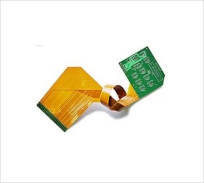
PCB surface treatment
There are many PCB surface treatment processes, such as hot air leveling, organic solderability protectant (OSP), full-plate nickel-plated gold, immersion gold, immersion tin, immersion silver, chemical nickel-palladium gold, and electroplated hard gold. The process, the following will be introduced one by one
1, hot air leveling (spray tan)
The general process of the hot air leveling process is micro-etching→preheating→coating flux→spraying→cleaning.
Hot air leveling, also known as hot air solder leveling (commonly known as spray tin),
is a process of applying molten tin (lead) solder on the surface of the PCB and flattening (blown) with heated
compressed air to form a layer that is resistant to copper oxidation. It also provides a good solderability coating.
When the hot air is leveled, the solder and copper form a copper-tin intermetallic compound at the junction.
The PCB is sunk in the molten solder during hot air leveling; the air knife blows the liquid solder before the solder solidifies; the air knife minimizes the meniscus of the solder on the copper surface and prevents solder bridging.
Hot air leveling is divided into vertical type and horizontal type. It is generally considered that the horizontal type is better, mainly because the horizontal hot air leveling coating is relatively uniform and can realize automatic production.
Advantages: Long storage time; after the completion of the PCB, the copper surface is completely wetted (completely covered with tin before soldering); suitable for lead-free soldering; mature technology, low cost, suitable for visual inspection and electrical measurement
Disadvantages: Not suitable for wire bonding; due to surface flatness problems, there are limitations in SMT; it is not suitable for contact switch design. Copper will dissolve when tin is sprayed and the board will experience a high temperature. Particularly thick or thin plates, the tin spray has limitations, and production operations are inconvenient.
2. Organic solderability protector (OSP)
The general process is decreasing -> micro-etching -> pickling -> pure water cleaning -> organic coating -> cleaning, process control is relatively easy to show relative to other processes.
OSP is a process that meets the requirements of the RoHS Directive for printed circuit board (PCB) copper foil surface treatment.
OSP is the abbreviation of Organic Solderability Preservatives. Chinese translation is an organic solder mask,
also known as a copper protector. It is also known as Preflux in English. Simply put, OSP chemically grows an organic film on a clean bare copper surface. This film has anti-oxidation, thermal shock resistance, and moisture resistance. It is used to protect the copper surface from rust (oxidation or vulcanization) in the normal environment. However, in the subsequent high temperature of welding, the protective film must be very It is easily removed by the flux so that the exposed clean copper surface can be immediately combined with the molten solder into a firm solder joint in a very short time.
Advantages: Simple process, very flat surface, suitable for lead-free soldering and SMT. Easy to rework, easy to produce and operate, suitable for horizontal operation. The board is suitable for multiple processes (eg OSP+ENIG). Low cost and environmentally friendly.
Disadvantages: Restriction of the number of reflows (multiple welds are thick, the film will be destroyed, basically no problem 2 times). Not suitable for crimping technology, wire bonding. Visual inspection and electrical measurement are inconvenient. N2 gas protection is required for SMT. SMT rework is not suitable. Storage conditions are high.
3, full plate nickel-plated gold
Nickel plated gold is plated with a layer of nickel on the surface conductor of the PCB and then plated with a layer of gold.
The nickel plating is mainly to prevent the diffusion between gold and copper. There are two types of electroplated nickel-gold: gold-plated gold (pure gold, the gold surface does not look bright) and hard gold (the surface is smooth and hard, wear-resistant, contains other elements such as cobalt, and the gold surface looks brighter). Soft gold is mainly used for gold wire bonding in chip packaging; hard gold is mainly used for electrical interconnection in non-welded parts.
Advantages: Long storage time >12 months. Suitable for contact switch design and gold wire bonding. Suitable for electrical testing
Weakness: Higher cost, gold is thicker. Additional design lines are required to conduct electricity when plating gold fingers. Because the thickness of gold is not always applied, when it is applied to the welding, the solder joint may be embrittled due to too thick gold, which may affect the strength. Plating surface uniformity issues. The plated nickel-gold does not wrap the edges of the wire. Not suitable for aluminum wire bonding.
4, Shen Jin
The general process is deacidification cleaning -> micro-etching -> prepreg -> activation -> electroless nickel plating -> chemical immersion gold; there are 6 chemical tanks in the process, involving nearly 100 kinds of chemistry Product, the process is more complicated.
Shen Jin is a thick, electrically good nickel-gold alloy wrapped on the copper surface, which can protect the PCB for a long time;
it also has environmental tolerance not available in other surface treatment processes.
In addition, immersion gold can also prevent the dissolution of copper, which will benefit lead-free assembly.
Advantages: It is not easy to oxidize, can be stored for a long time, and the surface is flat. It is suitable for soldering fine gap pins and components with small solder joints. The first choice for a button PCB board (such as a mobile phone board). Reflow soldering can be repeated multiple times and it is less likely to reduce solderability. Can be used as a substrate for COB (Chip On Board) wire bonding.
Disadvantages: high cost, poor soldering strength, because of the use of electroless nickel process, easy to have black disk problems. The nickel layer oxidizes over time and long-term reliability is a problem.
5, Shen Xi
Since all current solders are based on tin, the tin layer can be matched to any type of solder. The immersion tin process can form a flat copper-tin intermetallic compound. This property makes the immersion tin have the same good solderability as the hot air leveling without the hot air leveling headache. The slab cannot be stored for too long. The assembly must be carried out according to the order of the tin.
Advantages: Suitable for horizontal production. Suitable for fine line processing, suitable for lead-free soldering, especially suitable for crimping technology. Very good flatness, suitable for SMT.
Disadvantages: Good storage conditions are required, preferably no more than 6 months to control tin whisker growth.
Not suitable for contact switch design. The process requirements for the solder mask process are relatively high,
otherwise, the solder mask will fall off. When welding multiple times, it is best to protect with N2 gas.
Electrical measurement is also a problem.
6, Shen Yin
The silver process is between organic coating and electroless nickel/immersion gold. The process is relatively simple and fast.
Even if exposed to heat, humidity, and pollution, silver can maintain good solderability, but it will lose its luster.
Silver does not have the good physical strength of electroless nickel/immersion gold because there is no nickel under the silver layer.
Advantages: Simple process, suitable for lead-free soldering, SMT. The surface is very flat, low cost and suitable for very fine lines.
Disadvantages: High storage requirements and easy contamination. The welding strength is prone to problems (micro-cavity problems). It is prone to electromigration and the occurrence of Giovanni bite in the copper under the solder mask. Electrical measurement is also a problem
7. Chemical nickel palladium gold
Compared with immersion gold, chemical nickel-palladium gold has an additional layer of palladium between nickel and gold. Palladium can prevent corrosion caused by displacement reaction and is fully prepared for immersion gold. Gold is tightly covered on top of the palladium to provide a good contact surface.
Advantages: Suitable for lead-free soldering. The surface is very flat and suitable for SMT. The through holes can also be nickelized. Long storage time, storage conditions are not critical. Suitable for electrical testing. Suitable for switch contact design. Suitable for aluminum wire binding, suitable for thick plates, strong against environmental attacks.
8, electroplated hard gold
In order to improve the wear resistance of the product, the number of insertions and removals is increased and the hard gold is plated.
The surface treatment process of PCBs is not very big, it seems to be a distant thing, but it should be noted that long-term slow changes will lead to huge changes. As the environmental protection calls are getting higher and higher, the surface treatment process of PCBs will definitely change dramatically in the future.
Alice Lu,
Eamil: sales16@andwinpcb.com