- Single-sided PCB process flow:
Blanking → screen printing → etching → removal of printing materials → hole processing → printing mark → coated flux → finished product.
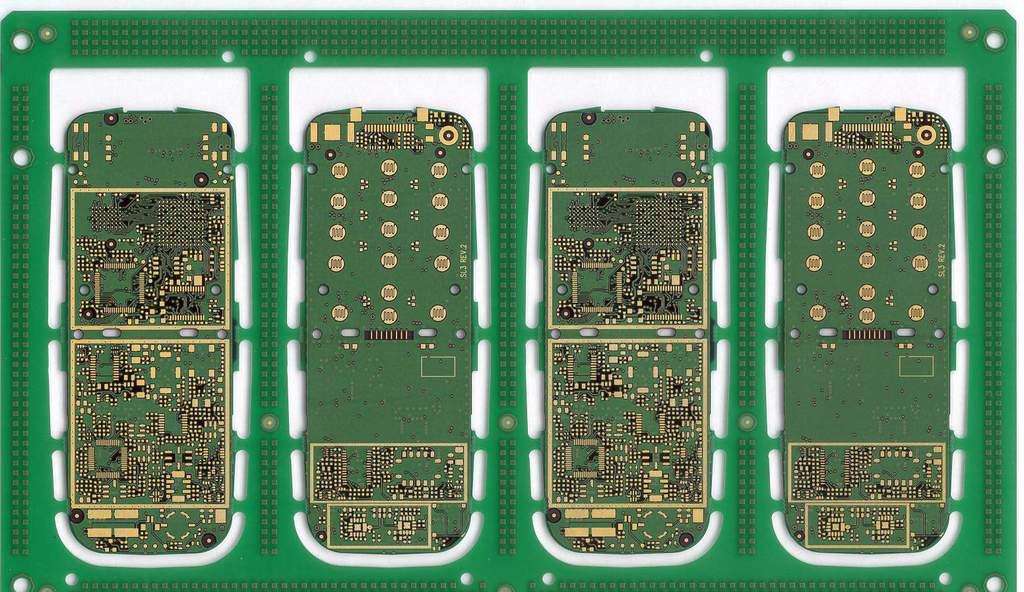
- The process flow of multilayer printed boards:
Inner Material Processing → Positioning Hole Machining → Surface Cleaning → Inner Layer Traces and Patterns → Corrosion → Laminate Pretreatment → Outer Inner Layer Material Lamination → Hole Machining → Hole Metallization → Finger Outer Layer Pattern → Plating Resistant to Corrosion Weldable metal → removal sensation → photo-resist corrosion → plug gold plating → profile processing → hot-melt → coating flux → finished product.
Printed Circuit Board Features
Printed circuit boards have the following functions in electronic devices:
Provides mechanical support for fixing and assembling various electronic components such as integrated circuits, wiring, and electrical connection or electrical insulation between various electronic components such as integrated circuits, and provides required electrical characteristics.
Provides solder mask patterns for automatic soldering, providing identification characters and graphics for component insertion, inspection, and repair.
After the electronic equipment adopts the printed board, due to the consistency of the same type of printed board, manual wiring errors can be avoided, and automatic assembly or mounting of electronic components, automatic soldering, and automatic detection can be realized, thereby ensuring the quality of electronic products. Increased labor productivity, reduced costs, and ease of maintenance.
Printed circuit board development trend
PCBs have evolved from single layers to double-sided, multi-layered, and flex-boards, and have continued to develop with high precision, high density, and high reliability. Continually shrinking the volume, reducing the cost, and improving the performance, the printed board still maintains a strong vitality in the future development of electronic products.
In the future, the development trend of PCB manufacturing technology is to develop high-density, high-precision, fine-pore diameter, fine conductive wire, small pitch, high reliability, multi-layered, high-speed transmission, lightweight, and thin type in performance.
Alice Lu
My Email: sales16@andwinpcb.com