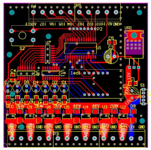
What is the meaning of layers in the PCB?
The meaning of layers in the PCB
Signal Layers:
Signal layers include Top Layer, Bottom Layer, and Mid Layer 1…30.
These layers are all layers with electrical connections, that is, the actual copper layers.
The middle layer refers to the middle board layer used for wiring. The layer is covered with wires.
Top Layer.
The top layer, also called the component layer, is mainly used to place components.
For double layers and multilayers, it can be used to arrange wires or copper.
Bottom signal layer (Bottom Layer), also known as solder layer, is mainly used for wiring and soldering. For double-layer board and multilayer board, components can be placed.
Mid-Layers can have up to 30 layers and are used to arrange signal lines in the multilayer board.
This does not include power lines and ground lines.
Internal Plane:
Internal Plane 1…16, this type of layer is only used for multi-layer boards.
These layers are generally connected to ground and power.
They become the power and ground layers.
They also have electrical connections and are also actual copper. Layer,
but this layer is generally not covered by the wiring and consists of a whole piece of copper film.
Usually referred to as the inner layer, it only appears in the multilayer board. The number of PCB layers generally refers to the sum of the signal layer and the inner layer.
Similar to the signal layer, the internal electrical layer and the internal electrical layer, and the internal electrical layer and the signal layer may be connected to each other through a through hole, a blind hole, and a buried hole.
Silkscreen Overlay:
includes a top overlay and a bottom overlay. The silkscreen characters that define the top and bottom layers are some of the textual symbols typically printed on the solder mask, such as component names, component symbols, component pins, and copyrights, to facilitate future circuit soldering and troubleshooting.
A PCB board can have a maximum of 2 silk screen layers, namely Top Overlay and Bottom Overlay,
Which is generally white. It is mainly used to place printed information, such as contours and labels of components.
A variety of annotation characters, etc., to facilitate PCB components welding and circuit inspection.
The Top Overlay layer is used to label the component’s projection profile, the component’s label, nominal value or model number, and various comment characters. The Bottom Overlay is the same as the top screen layer.
If all the labels on the top layer are included, the bottom layer can be closed.
Paste Mask:
The solder paste layer, which includes the top paste layer and the Bottom paste layer,
refers to the exposed surface mount pads that we can see.
It is the part that needs to be coated with solder paste before welding.
Therefore, this layer is also useful when the pad is hot-air leveled and welded stencils are made.
Mechanical Layers:
Up to 16 mechanical layers can be selected.
Designing a double panel requires only the default option Mechanical Layer 1.
The mechanical layer is the definition of the appearance of the entire PCB board,
it is generally used to place the instructional information on the board and assembly methods,
such as the PCB’s dimensions, dimensions, data, information, PCB assembly instructions and other information.
Designed as a PCB mechanical shape, the default LAYER1 is the outline layer.
Other LAYER2/3/4 can be used as mechanical dimensioning or special purpose.
For example, LAYER2/3/4 can be used when some boards need to make conductive carbon oil,
but the use of this layer must be clearly marked on the same layer.
Mask Layers Altium Designer provides two types of mask layers, Solder Mask and Paste Mask,
with two layers, the top layer and the bottom layer.
Keep Out Layer:
Defines the boundaries of the wiring layer.
After defining the disabling of the wiring layer, the wiring with the electrical characteristics cannot exceed the boundary of the disabling wiring layer in the subsequent wiring process.
Many designers also use the mechanical shape of the PCB.
If there are KEEPOUT and MECHANICAL LAYER1 on the PCB, the appearance of the two layers is mainly determined by the appearance of MECHANICAL LAYER1.
It is recommended to use MECHANICAL LAYER1 as the outline when designing.
If using KEEPOUT LAYER as the outline, do not use MECHANICAL LAYER1 again to avoid confusion!
Drill Layer:
Drill guide and Drill drawing are drilling data.
Drilling layers provide drill hole information during the board manufacturing process (eg, pads, which require drilling).
Protel 99 SE provides two drilling layers, Drill gride and Drill drawing.
Multi-layer:
refers to all layers of the PCB board.
The pads on the circuit board and through-holes penetrate the entire circuit board and establish electrical connections with different conductive pattern layers.
Therefore, the system specifically sets up an abstract layer—multilayer.
In general, the pads and vias should be placed on multiple layers. If this layer is closed, the pads and vias cannot be displayed.
Solder mask:
Solder mask refers to the green oil part of the board; because it is a negative output,
so actually the actual effect of the solder mask part is not on the green oil, but the tin plating, silvery white!
The solder mask:
paste mask, which is used when the device is mounted on a chip.
It is the pad corresponding to all the patch components.
The size is the same as that of the toplayer/bottomlayer layer.
It is used to open the steel mesh for tin leakage.
Grace Zheng
Email: sales06@andwinpcb.com
Other ,you may interesting

