The most complete summary of PCB surface finished process
The most basic purpose of PCB surface finished is to ensure good solderability or electrical properties. Since copper in nature tends to exist in the form of oxides in the air, it is unlikely to remain as raw copper for a long time, so other treatments of copper are required.
1, hot air leveling (spray tin)
Hot air leveling, also known as hot air solder leveling (commonly known as spray tin), is a process of applying molten tin (lead) solder on the surface of the PCB and flattening (blown) with heated compressed air to form a layer that is resistant to copper oxidation. It also provides a good solderability coating. When the hot air is leveled, the solder and copper form a copper-tin intermetallic compound at the junction. The PCB is sunk in the molten solder during hot air leveling; the air knife blows the liquid solder before the solder solidifies; the air knife minimizes the meniscus of the solder on the copper surface and prevents solder bridging.
2,Organic solderability protector (OSP)
OSP is a process that meets the requirements of the RoHS Directive for printed circuit board (PCB) copper foil surface treatment. OSP is the abbreviation of Organic Solderability Preservatives. Chinese translation is organic solder mask, also known as copper protector. It is also known as Preflux in English. Simply put, OSP chemically grows an organic film on a clean bare copper surface. This film has anti-oxidation, thermal shock resistance and moisture resistance. It is used to protect the copper surface from rust (oxidation or vulcanization) in the normal environment. However, in the subsequent high temperature of welding, the protective film must be very It is easily removed by the flux, so that the exposed clean copper surface can be immediately combined with the molten solder into a firm solder joint in a very short time.
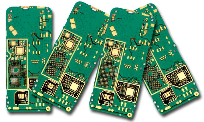
3, full plate nickel-plated gold
Nickel plated gold is plated with a layer of nickel on the surface conductor of the PCB and then plated with a layer of gold. The nickel plating is mainly to prevent the diffusion between gold and copper. There are two types of electroplated nickel gold: gold-plated gold (pure gold, the gold surface does not look bright) and hard gold (the surface is smooth and hard, wear-resistant, contains other elements such as cobalt, and the gold surface looks brighter). Soft gold is mainly used for gold wire bonding in chip packaging; hard gold is mainly used for electrical interconnection in non-welded parts.
4, Shen Jin
Shen Jin is a thick, electrically good nickel-gold alloy wrapped on the copper surface, which can protect the PCB for a long time; it also has environmental tolerance not available in other surface treatment processes. In addition, immersion gold can also prevent the dissolution of copper, which will benefit lead-free assembly.
5, Shen Xi
Since all current solders are based on tin, the tin layer can be matched to any type of solder. The immersion tin process can form a flat copper-tin intermetallic compound. This property makes the immersion tin have the same good solderability as the hot air leveling without the hot air leveling headache. The slab can not be stored for too long. The assembly must be carried out according to the order of the tin.
6, Shen Yin
The silver process is between organic coating and electroless nickel/immersion gold. The process is relatively simple and fast. Even if exposed to heat, humidity and pollution, silver can maintain good solderability, but it will lose its luster. . Silver does not have the good physical strength of electroless nickel/immersion gold because there is no nickel under the silver layer.
7,Chemical nickel palladium gold
Compared with immersion gold, chemical nickel-palladium gold has an additional layer of palladium between nickel and gold. Palladium can prevent corrosion caused by displacement reaction and is fully prepared for immersion gold. Gold is tightly covered on top of the palladium to provide a good contact surface.
8, electroplated hard gold
In order to improve the wear resistance of the product, the number of insertions and removals is increased and the hard gold is plated.
Grace Zheng
Email: sales06@andwinpcb.com