10 layer pcb stackup
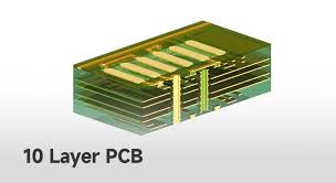
1.What is 10-layer pcb
A 10-layer printed circuit board (PCB) is a sophisticated and highly functional component used in various advanced electronic applications. Understanding its structure, benefits, and applications is crucial for those involved in electronics design and manufacturing. The complexity of a 10-layer PCB lies in its multiple layers of conductive and insulating materials, which are meticulously arranged to achieve optimal performance and reliability.
2.What is the structural composition of a 10-layer PCB?
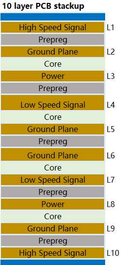
The structure of a 10-layer PCB consists of ten distinct layers, including signal layers, power planes, and ground planes. These layers are laminated together using insulating materials such as prepreg and core, which provide electrical insulation and mechanical support. The signal layers are responsible for carrying electrical signals between different components on the board, while the power and ground planes distribute power and provide a reference voltage, respectively. The arrangement of these layers is carefully designed to minimize electromagnetic interference (EMI) and ensure signal integrity

GET PCB MANUFACTURING AND ASSEMBLY QUOTE NOW!
3.What are the advantages of 10-layer PCB?
(1)support complex and high-density designs.
(2)offer enhanced thermal management capabilities
(3)contribute to overall product miniaturization
(4)support high-density interconnections
(5) The multiple layers provide more surface area for heat dissipation, which is essential for maintaining the reliability and longevity of electronic components.
4.What are the disadvantages of 10-layer PCB?
(1)increased cost
(2)increased design time and effort required
(3)The risk of defects such as misalignment, delamination, or incomplete connections increases with the number of layers.
One of the primary advantages of a 10-layer PCB is its ability to support complex and high-density designs. With multiple layers, designers can incorporate more components and intricate circuitry within a limited space.
This is particularly beneficial for advanced electronic devices such as smartphones, computers, and medical equipment, where space is at a premium and performance requirements are stringent. The additional layers allow for better signal integrity and reduced electromagnetic interference (EMI), which are critical for maintaining the reliability and efficiency of high-speed circuits.
Moreover, 10-layer PCBs offer enhanced thermal management capabilities. The multiple layers can be used to distribute heat more effectively, preventing hotspots that could potentially damage components or degrade performance.
This is especially important in applications that generate significant amounts of heat, such as power electronics and high-performance computing systems.
By incorporating dedicated ground and power planes, a 10-layer PCB can also improve power distribution and reduce voltage drops, ensuring stable operation of the entire system.
In addition to these technical benefits, 10-layer PCBs can contribute to overall product miniaturization.
As electronic devices continue to shrink in size, the ability to pack more functionality into a smaller footprint becomes increasingly valuable.
A 10-layer PCB can help achieve this by allowing for more compact and efficient designs, which can lead to lighter and more portable end products.
However, despite these advantages, there are also notable disadvantages associated with 10-layer PCBs. One of the most significant drawbacks is the increased cost.
The complexity of manufacturing a 10-layer PCB is considerably higher than that of a simpler, lower-layer board. This complexity translates into higher production costs, which can be a limiting factor for budget-conscious projects or for products that need to be produced in large volumes.\
Another disadvantage is the increased design time and effort required.
Designing a 10-layer PCB demands a higher level of expertise and meticulous planning to ensure that all layers are correctly aligned and that signal integrity is maintained throughout the board.
This can lead to longer development cycles and may require specialized design tools and software, further adding to the overall cost and complexity.
Additionally, the manufacturing process for 10-layer PCBs is more challenging and prone to errors. The risk of defects such as misalignment, delamination, or incomplete connections increases with the number of layers.
This necessitates rigorous quality control measures and thorough testing, which can further extend production times and costs.
GET PCB AND ASSEMBLY SERVICE QUOTE NOW!
5.Application of 10-layer PCB
(1)used in various high-speed digital systems
(2)telecommunications equipment
(3)high data centers
(4)advanced driver-assistance systems
(5) aerospace and defense
he versatility of a 10-layer PCB makes it suitable for a wide range of applications.
In the telecommunications industry, these PCBs are used in networking equipment, base stations, and other communication devices that require high-speed data transmission and reliable performance.
In the aerospace and defense sectors, 10-layer PCBs are employed in avionics, radar systems, and other mission-critical applications where reliability and durability are paramount. Additionally, the medical industry relies on 10-layer PCBs for advanced diagnostic and monitoring equipment, where precision and accuracy are essential.