Copper coin pcb is excellent embedded copper coin technics for thermal management
What is copper coin PCB?
The technological evolution has made things more advanced.
The devices are becoming smart and multifunctional with large-scale integration ,
To increase the anticipation of rapid heat dissipation in Printed Circuit Boards (PCBs).
It is highly recommended for its increasing interconnection density as stable electrical performance,
And reliability while performing in high-power operation.
Intensive drilling of holes and local thick copper plating along with local thick copper plating,
That induced in PCB manufacturing that helps in thermal management.
It has a disadvantage that the interconnection density ,
It will be limited in designs with increasing holes and copper plating areas.
Controlling the heat loss of electronic and microelectronic systems is quite challenging.
PCBs by nature are not a good option for the thermal conductor.
Therefore, the thermal conductivity of typical substrate material is necessary
And copper is the perfect material in this regard.
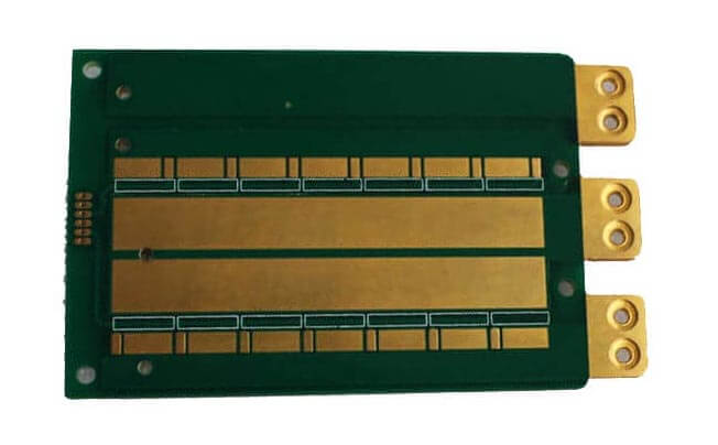
Copper coin PCB comprises the conductive traces of a PCB with high thermal conductivity.
The copper coin PCB
To keep pace with technological advancement,
Thermal management has become a crucial issue at the bare PCB and assembly level.
It is essential for brightening LED applications,
High power transmitters as well as in high voltage power supplies.
This needs a solution with the uprising demand for better heat transfer and ,
Cooling compatibility and the solution is the Copper Coin PCB.
The copper coin PCB is made with a layer of high-quality copper foil covered,
And with insulating material with a substrate.
It delivers mechanical support and makes a connection to the electronic components seamlessly.
The materials are induced by electrically conductive pads and tracks,
It is to connect the electronic components with security.
PCB copper coins are used for heat dissipation at first.
The evolution of electronic devices and the emergence of tiny electronic circuits ,
It required a high heat dissipation solution with extended capacity in PCB.

Copper coin PCB technology evolving
The technology is evolving for the copper coin PCBs.
It is highly efficient for heat dissipation that occurs at a higher rate ,
And with high thermal conductive materials.
Copper offers upwards of 400W/m.K thermal conductivity,
It is compared to other materials that can manage the heat at the same
time keeping electrical and thermal conductivity intact.
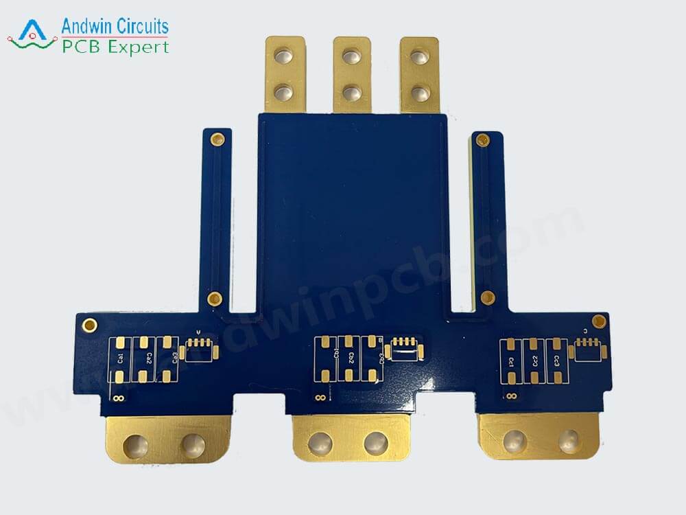
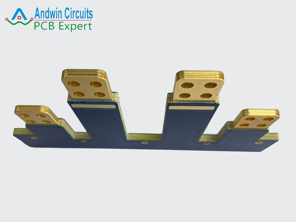
The copper coin PCB is made of a simple piece of solid copper.
It is inserted into the PCB under the components for cooling.
The copper coin has more cooling compatibility than the others via farm.
It has direct connect with the heat-generating compounding pad,
That enables a heat sink.
The thermal conduciveness of copper is 30 to 200 times better,
That compared to any conductive dielectric prepreg.
For a specific or small number of components on a PCB,
copper coin technology is the best-suited solution ,
Because of its extraordinary heat management.
The concept of multi-layer PCB is regardless of its localized fashion that is based
on a copper coin press.
It fits into a premade cutout in the board that sits right under the hot spot.
It transfers the heat directly to the heat sink through the PCB stack-up.
Once the copper coin is inserted into the PCB,
It can incorporate in different forms and configurations,
That are chosen by the designers.
It reflects the trade-off between routing, power plane requirement,
and proximity of the copper coin to the component that is needed for cooling.
Though the technology of copper coin PCBs is relatively new and the success
ratio is quite high compared to other PCBs, It is because of its optimal design.
You can include it whenever you require,
Especially while putting a foreign object into a stack-up, registration,
And tolerance becomes a bigger concern.
It has a greater need for process control that makes it highly efficient.
Importance of using Copper Coin PCB
The copper coin embedded in the PCB slot resides after routing and metal greased to finish PCB lamination,
Make sure the PCB and the copper coin are connected tightly.
Traditionally the heat dissipation was designed in PCB through thermal vias holes.
The majority of the PCB materials are not good for heat transfer,
And some crucial components require greater performance in terms of heat dissipation.
The standard via holes is mostly unable to meet these requirements.
In this regard, copper offers an excellent conductor of heat ,
And therefore the demand is increasing in the market for active PCBs.
The PCB embedded coin technology lets you insert a copper coin directly into the board.
The component will absorb and dissipate excess heat.
Multiple shapes of these coins are used depending on the area to offset the excess heat.

Types of Copper Coin PCB
The Coin technology has been developed to enhance heat dissipation from high
power components to a cooling fin that is stated at the back of the board.
This helps to enhance the reliability of the components and makes them durable.
The coin can be also used conduction in the circuit and,
The technology is inducive for greater thermal and electric transmission ,
To achieved at low cost and relatively simple in processing.
Based on the processing criteria of copper coin PCB,
It is found in two types:
1. Embedded Copper Coin PCB:
The copper coin is inserted into the PCB slot after routing
And metalizing have been done in the PCB press.
It will remain tightly connected with copper coins
Through the embedding quantity between them.
The electrical connection is achieved by copper plating.

2. Buried Copper Coin PCB:
It keeps the copper coin buried into the pre-milling groove,
while pressing and connected by laminated prepreg.
In this type of PCB,the copper coin remains hidden in the pre-milling groove during pressing.
Currently, many ways have been evolved to solve the PCB heat dissipation problem.
For example, dense heat dissipation hole design, thick copper foil
circuit, metal-based (core) structure, embedded copper coin design,
copper-based convex design, high thermal conductivity materials, and so on.
The embedded copper coin PCB is the most effective and efficient way to solve the problem of extreme heat dissipation.

Embedded Copper Coin PCB
The embedded copper coin PCB is the one that is widely useful,
That used for various purposes to meet the heat dissipation requirements,
As well as for the high-power components.
It comprises high thermal conductivity in copper coins.
When the connection with the PCB,
It can be divided into buried copper coin PCB,
And embedded copper coin PCB.
The thickness of embedded copper coins are two types, such as:
- Un-stacked copper coin
- Stacked copper coin
The PCB-embedded copper coin has a direct connection with the inner copper layer and air, heat transfers to the copper coin quickly when PCB is used.
The heat is then removed from the air through the copper coin.
The development of new-generation information technology:

Buried Copper Coin PCB
The embedded copper coin makes direct contact with the inner copper layer and air.
It transfers heat to the copper coin as soon as the PCB is in use.
After that, the heat is been removed from the air through the copper coin.
The buried copper coin PCB is pressed and connected,
It is laminated in prepreg formulabut,
And is not effective enough for heat conduciveness.
Buried copper coin PCBs consume less cost and the processing is lower, but the application prospect is broad.
On the other hand, the embedded PCB technology is not mature and difficult
whereas buried copper coin PCB is working better and reliable.
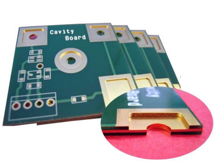
The thickness of the copper coin is thinner than PCB board thickness,
where the routing window the PCB board comprises with two copper coins,
Such as:
Cavity routing slot on the copper coin
No cavity routing slot on the copper coin

Extensive Thermal Solution
The type of copper coin PCB is required for a generic solution,
That depend on the designer,
Who has to determine the type of coin to embed in the particular PCB.
The appropriate copper coin in PCB requires proper routing and metallization for lamination,
That created tight connectivity among the PCB and the copper coin.
It is done through the electrical connection copper plating,
That results in superior heat dissipation performance.
We always call “embedding” that is opposed to “burying”,
Because it is buried in a copper coin and puts into a pre-milling groove while pressing connected by lamination.
To embed a copper coin is complex than the buried one.
The reliability is issued not performed by a well-trained engineer,
Even embedding is rapid and cost-effective as well.
It produces greater heat dissipation burying.
The Concurrent Design
Heat dissipation is the prime concern for Copper Coin PCBs that can be done in multiple ways.
Depending on the application type, the concurrent design is made.
It can be various types, such as:
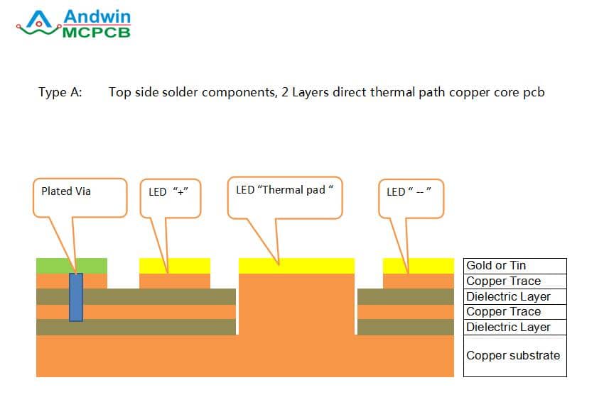
1. A solid copper path that flows from layer 1 to layer 4.
It is acted as the assembly pad and provides the ultimate heat transfer channel for a hot component.
For smaller pad sizes, the routing is considered to be under a hot pad so the copper coin can be pressed and fit only up to a designated layer.
It avoids passing through the entire PCB for certain reasons and is placed in between layer 4 and layer 2 without making any contact with layer 1.
2. Another design of the PCB can be a “T” shaped coin that makes it superior for using the properties of copper coin technology.
The heat generation pad or the heat sink can be different in areas and a small pad and larger heat sink or the other way around.
The limitations of a small copper coin PCB can be solved by using the “T” shaped coin.
It keeps the entire dimension of the copper coin at the minimum possible level and creates a contact within the pad smaller than the minimum copper coin size. This makes it easy to fulfill the size requirements with an excellent trade-off in terms of performance.
The shape also serves greater flexibility and occupies minimal space in the board.
Choose the exact shape is important and it is critical for copper coin PCB.
If the shape is poor, the design can result in damage to the groove wall, the coin, or both, and creates more waste for the manufacturing process.
The embedding can also fail if the coin is not shaper perfectly.
It is a key process that needs accurate dimension, smoothness, and other technical difficulties that is easy to produce reliability problems.
The shape and design affect the embedding effect of copper coin that results in damage to copper coin and groove wall.
The groove size also matters according to the base plate that is not consistent with the compensation design of the copper coin size.
It cannot be achieved the common wear of the copper coin and groove wall, lead to embedded copper coin, and substrate wall.
This cannot be closely contacted for the copper coin pushing force.
The smoothness of embedded copper coins comprises the flatness of copper coins that cannot meet the general requirements of component surface and welding surface.
It is leading to excessive height difference can be reduced by the heat dissipation effect of electronic components and copper coin.
For thermal transfer, Copper Coin is the pinnacle and it can be applied efficiently at the bare PCB level and can be extremely good for working on an MCPCB design or copper coin design.
The technical difficulties in the processing of the PCB products embedded in copper coin.
It is combined with various test results and production verification that is effectively improved the defects to groove wall damage, poor adhesion, and poor smoothness in the processing of PCB products embedded in copper coin.
High heat dissipation is crucial to make sure the PCBs perform their tasks perfectly.
High heat dissipation is required for the instant insertion of an embedded copper coin so that it can work faster with enhanced reliability.
Therefore, Copper Coin PCB has been emerged into the world of high-grade electronic devices to ensure greater performance with better heat dissipation

Thermal sink PCB
Andwin Circuits Co.,Limited
PCB and PCB assembly
Please send email: sales@andwinpcb.com ( priority ) with your PCB Gerber file Or/and BOM file to us,
Our teams will quote for you as soon as possible.
Or submit follow form our team will contact you soon.