Telecommunication PCB Manufacturing
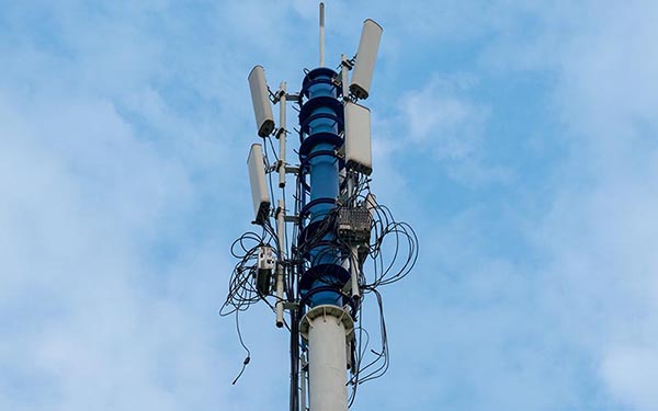
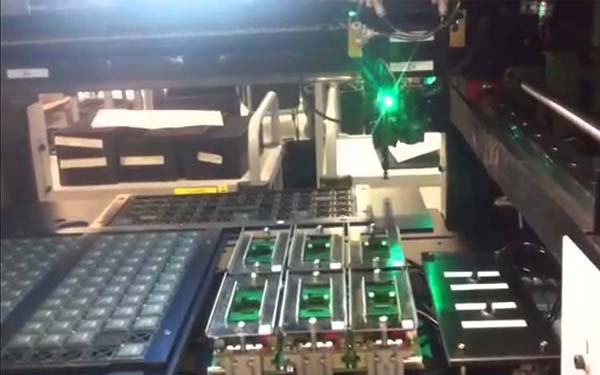
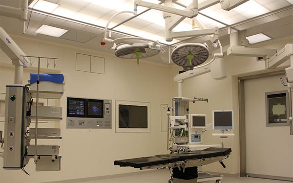
Telecommunication is the transmission of information over wire, radio, optical, or electromagnetic systems. As 5G networks and communication technology advance, high-performance PCBs are essential for modern infrastructure.
Andwin Circuits has specialized in telecommunications PCB manufacturing since 2003, delivering high-frequency and thermal management solutions for 5G base stations, radar systems, and fiber optic equipment.
Telecommunications PCB Solutions
1. 5G Base Station and Application
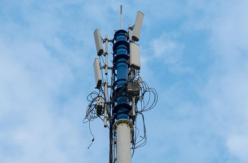
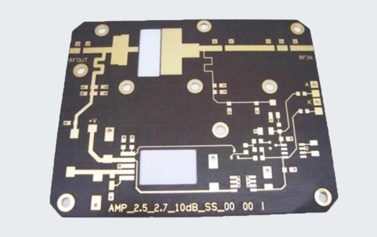
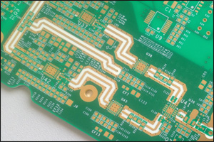
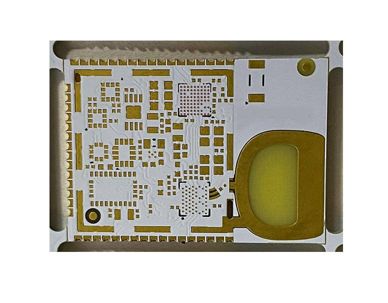
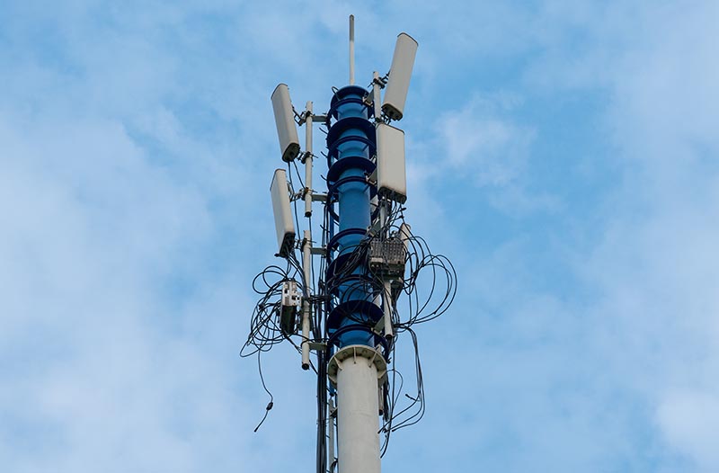
5G networks demand PCBs capable of handling millimeter-wave frequencies, massive MIMO arrays, and high-power radio units with ultra-low latency performance.
2. Microwave Radar
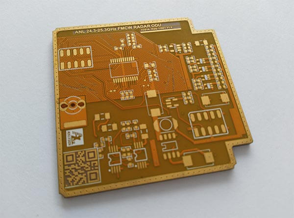
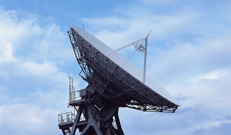
Radar systems demand PCBs that transmit and receive microwave signals with minimal loss and maximum precision for telecommunications, automotive, and industrial applications.
3. Photo-Communication
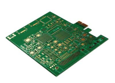
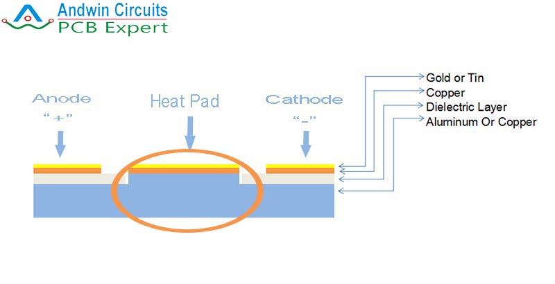
Fiber optic systems require effective thermal management for high-power laser drivers, optical transceivers, and wavelength division multiplexing (WDM) systems to maintain performance and component lifespan.
Why Choose Andwin Circuits
Manufacturing telecommunications PCBs since 2003 for leading equipment manufacturers worldwide.
Full range of high-frequency materials: Rogers, Taconic, Arlon, Isola, Megtron, ceramics. Expert material selection guidance.
±5% impedance control, 1-30+ layers, 3/3 mil trace/space, 0.1mm holes, 0.5-10 oz copper, boards up to 600x1200mm.
Rapid 24-72 hour prototypes, 5-7 day production. Strict ISO 9001:2015, IPC-6012 Class 3, RoHS/REACH compliant.
Frequently Asked Questions
What PCB materials are best for 5G base station applications?
For sub-6 GHz 5G, Rogers 4350B or Megtron 6 offer excellent performance at reasonable cost. For millimeter-wave 5G (24-100 GHz), Rogers 5880 or Taconic RF-35 are recommended due to their ultra-low loss characteristics and stable dielectric properties at high frequencies.
How do you ensure impedance control for high-frequency PCBs?
We use controlled impedance manufacturing processes including precise dielectric thickness control, copper weight management, and trace width/spacing verification. Every controlled impedance board is tested using time-domain reflectometry (TDR) to verify impedance within ±5% tolerance.
What is the lead time for telecommunications PCB manufacturing?
Standard lead time is 5-7 days for most telecommunications PCBs. We offer 24-72 hour expedited service for urgent prototypes. Volume production lead times are typically 10-15 days for orders over 1,000 pieces.
Can you manufacture mixed-stack PCBs with both FR4 and high-frequency materials?
Yes, we specialize in hybrid stack-ups combining cost-effective FR4 layers for power and digital circuits with high-frequency materials like Rogers for RF sections. This approach optimizes both performance and cost.
What thermal management options do you offer for photo-communication applications?
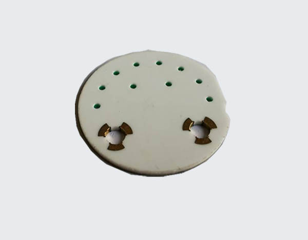
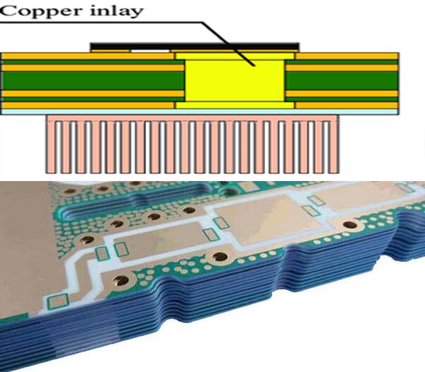
We offer multiple thermal management solutions: MCPCBs with aluminum or copper cores (up to 395 W/m/K), ceramic substrates (AlN, Al2O3) for premium applications, heavy copper PCBs (up to 10 oz), copper coin/inlay technology, and optimized thermal via design.
What is the minimum order quantity for telecommunications PCBs?
We accept orders from single prototypes to high-volume production runs with no minimum order quantity. We’re happy to manufacture even a single board for testing and development.
Get Started with Your Telecommunications PCB Project
Ready to discuss your telecommunications PCB requirements? Our experienced engineering team is here to help you select the right materials, optimize your design, and deliver high-quality PCBs on time and on budget.