Aluminium nitride ceramic PCB
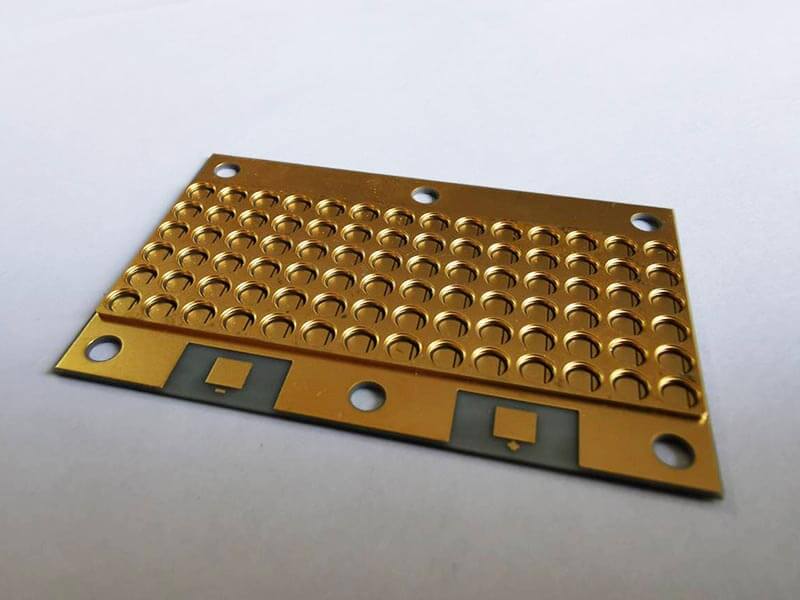
Aluminum Nitride Ceramic PCB substrate ( AlN ) is brown,
Thermal conductivity Min.275 W/m.k up to 320 W/m.k
Aluminum Nitride ceramic PCB substrate have better thermal conductivity,
Also,higher cost, choose a suitable material according your products.
It is important to choose the highly appropriate substrates for your electronic circuits.
There are different kinds of boards available,
but ceramic pcb get more fame among circuit board users because of its versatility.
If you want to get the best kinds of boards, you can contact us.
We offer the most reliable solutions based on the printed circuit boards requirements of
our customers.
The main reason to use these solutions is that they are ideal for all kinds of electronic
circuits which have minimal expansion coefficient and increased thermal conductivity.
With better versatility,
It appears as a perfect alternative to existing printed circuit board boasting of increased
performance and minimal complex design.
It ensures that ceramic pcb work effectively on chip-on-board modules, high-power circuits,
and proximity sensors.
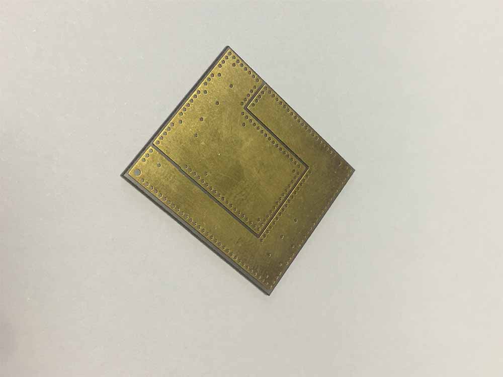
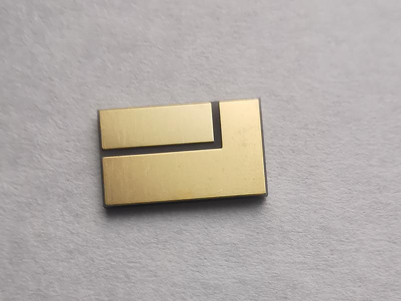
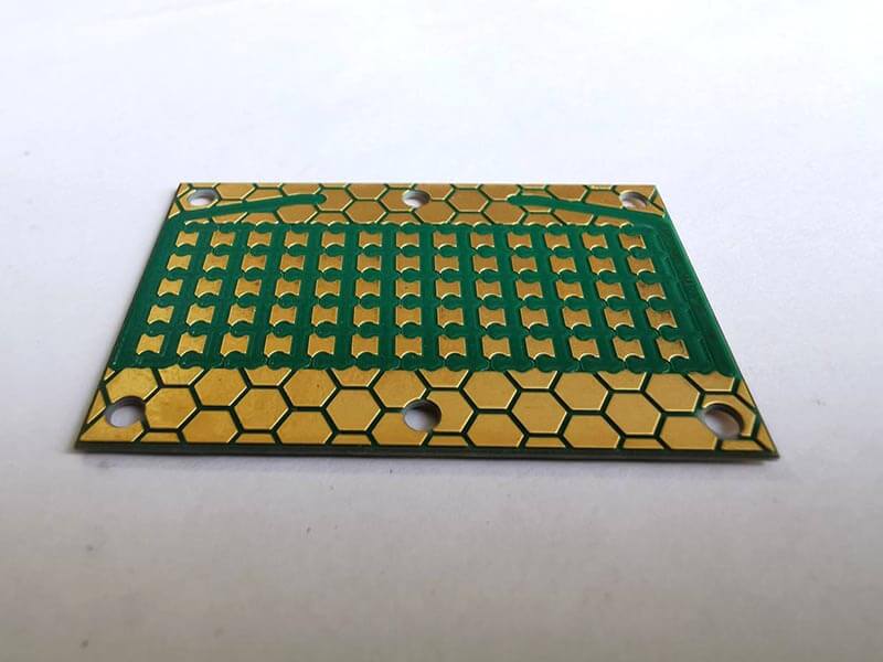
Aluminium nitride ceramic PCB capability
- Aluminum Nitride Ceramic ( AlN )
- Conductor: Copper (Cu) Silver ( Ag ) or Glod ( Au )
- Ceramic thickness: 0.25 | 0.38 | 0.50 | 0.635 | 0.76 | 1.0 |1.5 | 2.0 | 3.0mm
- Conductor thickness: 10um – 800um
- Min. Trace Space/width: 0.05 / 0.05mm ( 2 / 2 mil )
Aluminium nitride ceramic PCB application
- High power electronic semi-conductor module
- Injection System
- Anti-block Braking system
- High-power LED Chip
- Wafter Street light
- Fuel Sendor Resistor Card
- Electric power transmitter modules
- Solar cell
- Sensor
- Telecome device
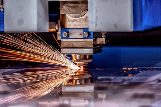
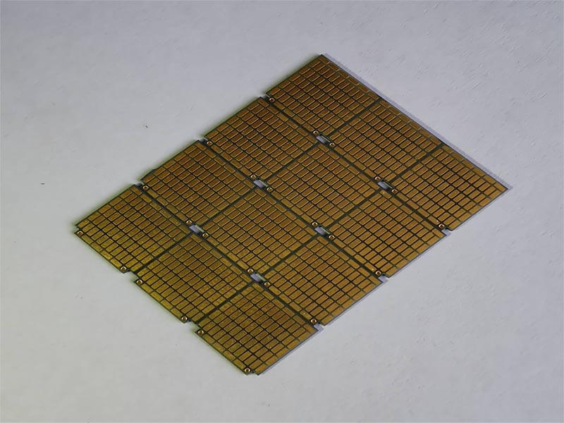
Only board with Rectrangle shape can be shipped via single piece, or via panel
Soldermask is also available upon request, working temperature >500 C,
and color is semi-transparent
Advantage of Aluminum Nitride Ceramic PCB
1. High thermal conductivity property and low thermal resistance,
Could increase the efficiency and operation lifetime of semi- conductor chips.
2. Excellent thermal cycling performance and fine mechanic strength.
3. High isolating strength
4. The thermal expansion coefficient is close to that of the silicon chip.
5. Strong current conductive ability
6. Fine environment compatiblity,no environment contaminative elements,
Such as PB,Hg and Cr,etc.
Be able to pass strict environment protection credentials.
Ceramic PCB
AIN ceramic PCB Sample
The famous brand ceramic PCB customers