DBC Ceramic PCB
Andwin Circuits builds DBC (Direct Bonded Copper) ceramic PCBs — copper foil is directly bonded to Al2O3 or AIN ceramic under high temperature for excellent electrical isolation, thermal conductivity and current-carrying capacity.
DBC Ceramic PCB Capability

DBC Ceramic PCB
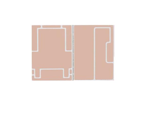
Direct Bonded Copper board

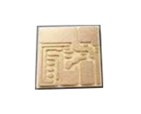
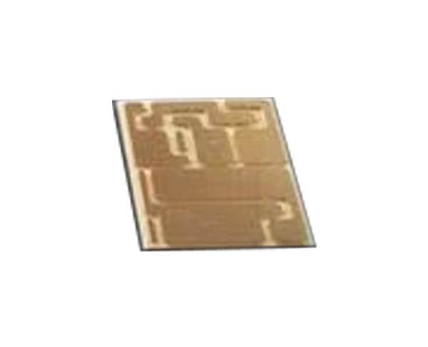
DBC Sample C110
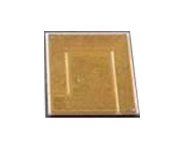
Finished board

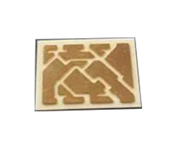
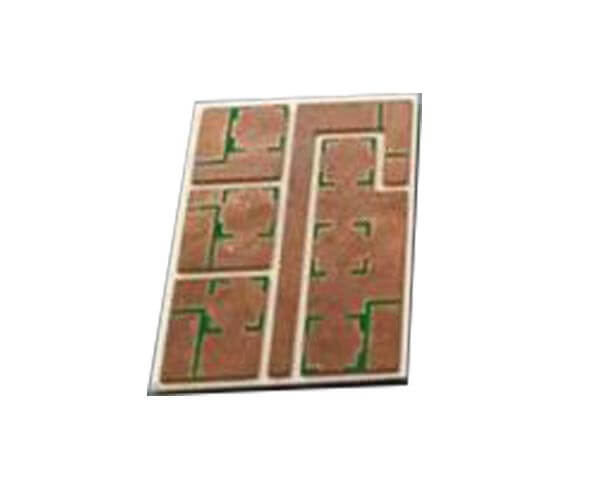
DBC Sample C113
Finished board

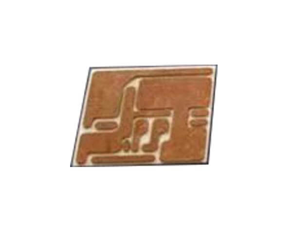
DBC Sample C114
Finished board.

DBC Sample C115
Finished board

DBC Sample C116
Finished board
Capability Parameters
Substrate material
Aluminum oxide Ceramic (Al2O3) 96% or 98%
Aluminum Nitride Ceramic ( AlN )
Max. board size
137 × 190 mm
Conductor
Copper
Ceramic thickness
0.38 | 0.50 | 0.635 | 0.76 | 1.0 | 1.5 | 2.0 mm
Copper thickness
Min. 105 µm ( 3 oz ), then 200 µm ( 0.2 mm ), 300 µm ( 0.3 mm ) or more
Min. trace space/width
0.2 / 0.2 mm ( 8 / 8 mil )
Why Choose DBC Ceramic PCB?
Excellent electrical isolation — ceramic substrate separates high-voltage copper layers reliably.
High thermal conductivity — heat leaves the chip straight through copper-bonded ceramic.
Fine solderability — copper surface takes standard soldering well.
High bonding strength — copper is directly bonded to ceramic, no adhesive to fail.
PCB-like structure / etched wiring — can be structured just like a PCB or get etched wiring.
High current loading capability — thick bonded copper carries high current with low loss.
Applications
High-power LED lighting fields where DTP MCPCB’s direct-bond cooling pays off .

IGBT module
Power semiconductor modules.

LED modules
High-power LED packages.

Solar cell
Photovoltaic electronics.

Electric power transmitter modules
Power conversion & transmission.

Sensor
Sensing electronics.
Frequently Asked Questions
1. What does DBC stand for?
DBC means Direct Bonded Copper — a technique where copper foil and Al2O3 or AIN ceramic (single or double sided) are directly bonded under high temperature, with no adhesive layer between them.
2. What ceramic materials are supported?
The source page lists Aluminum oxide Ceramic (Al2O3) 96% or 98% and Aluminum Nitride Ceramic (AIN) as the supported substrates.
3. What are the size and copper limits?
Max board size 137 × 190 mm; ceramic thickness from 0.38 to 2.0 mm; copper thickness min. 105 µm (3 oz) up to 200 / 300 µm or more; min. trace space/width 0.2 / 0.2 mm (8/8 mil).
4. Where are DBC ceramic PCBs used?
Per the source page: IGBT module, LED modules, Solar cell, Electric power transmitter modules, Sensor and other high temperature electronic products.
5. How do I get a quote?
Send your PCB Gerber file and/or BOM to sales@andwinpcb.com (priority). Our team will quote as soon as possible, or you can submit the on-page form and we will contact you.
Other PCB Products, You May Interest
Get professional one stop PCB solution from us!
Our engineering team provides free DFM analysis and design support.