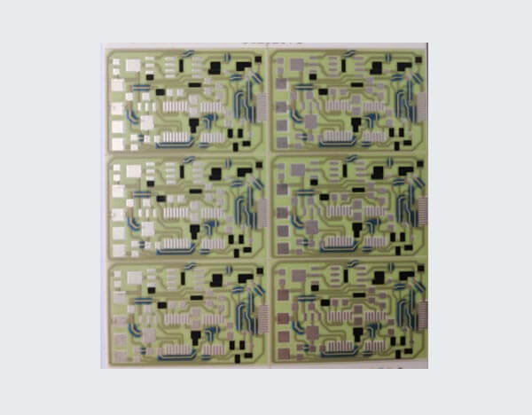
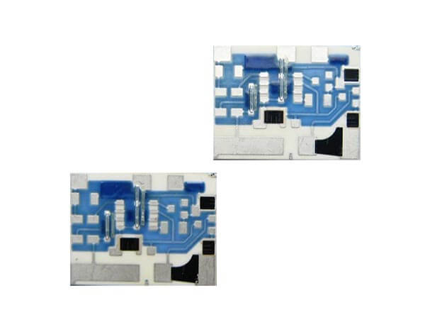
Thick film Ceramic PCB
Thick film ceramic pcb , ceramic Al2O3 AIN Beryllium Oxide (BeO)
Thick film ceramic pcb is use high temperature sintering technical,
To make conductor layer on Ceramic,
General the conductor layers are silver ( Ag ) or Glod( Au ).
Thickness of conductor layer 10um, around 10 – 13um , Max. 20um
Using thick film technology, Andwin can put resistor,
Electric capacity, conductor, semi-conductor,
and interchangable conductor on ceramic board,
After manufacturing steps of printing and high temperature sintering.
We can make all the resistors with the same value,
Or different value for different resistor on the same board.
Thick film ceramic PCB capability
- Aluminum oxide Ceramic (Al2O3) 96% or 98%
- Aluminum Nitride Ceramic ( AlN )
- Beryllium Oxide (BeO)
- Conductor Silver ( Ag ) or Gold ( Au )
- Ceramic thickness: 0.25 | 0.38 | 0.50 | 0.635 | 0.76 | 1.0mm 1.5mm 2.0mm
- Conductor thickness: 10um – 13um, Max 20um
- Min. Trace Space/width: 0.1 /0.1mm ( 4/4 mil )
Thick film ceramic PCB application
- High power electronic semi-conductor module
- Injection System
- Anti-block Braking system
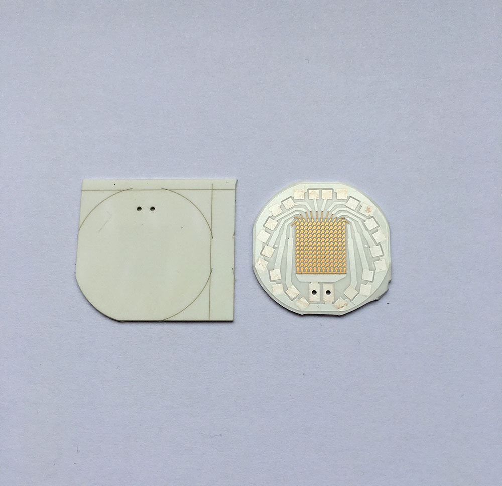
- High-power LED Chip
- Wafter Street light
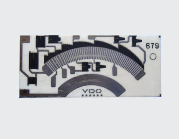
- Fuel Sendor Resistor Card
- Electric power transmitter modules
- Solar cell
- Sensor
- Telecome device
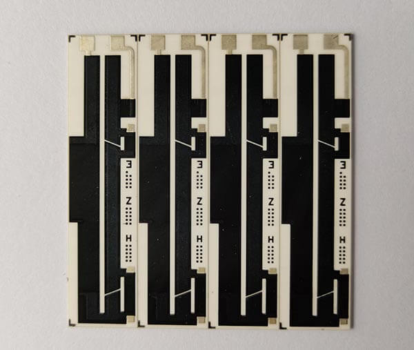
Only board with Rectrangle shape can be shipped via single piece, or via panel
Soldermask is also available upon request, working temperature >500 C,
and color is semi-transparent
For same stack up, cost lower than DBC Ceramic PCB, higher than MCPCB
Ceramic PCB
Thick film Ceramic PCB Sample
The famous brand ceramic PCB customers