IC Test Board
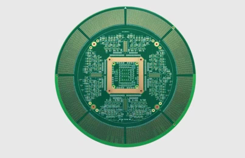
An Integrated Circuit (IC) test board is a specialized PCB that validates all functions of an IC before production integration. These boards require high layer counts, precision impedance control, and reliable connectivity for semiconductor testing and validation.
Andwin Circuits manufactures IC test board PCBs up to 36 layers with hard gold fingers, high Tg materials, and HDI technology for semiconductor manufacturers and testing laboratories.
IC Test Board PCB Solutions
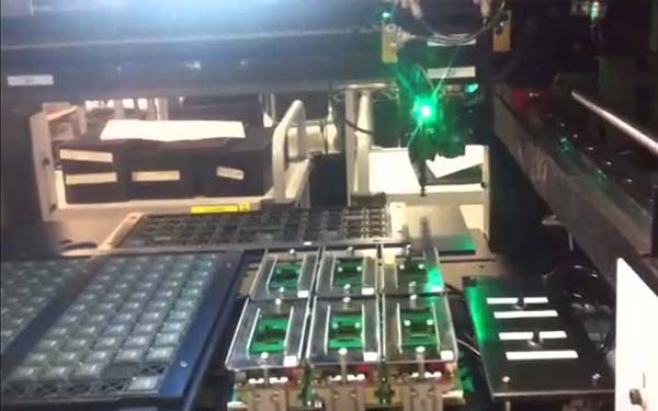
IC test boards require high layer counts, specialized materials, and durable connector finishes to validate semiconductor functionality through repeated testing cycles. Advanced materials and precision manufacturing ensure signal integrity and reliability.

Why Choose Andwin Circuits
Manufacturing IC test board PCBs since 2003 for semiconductor manufacturers, testing laboratories, and ATE equipment worldwide.
Up to 36 layers, HDI microvias, hard gold plating (30-50 micro-inch), controlled impedance ±5%, high Tg materials (>250°C).
IPC-6012 Class 3 standards, fine pitch down to 3/3 mil trace/space, via-in-pad capability, blind and buried vias, laser drilling.
24-72 hour prototypes, 5-10 day production for high layer count boards. ISO 9001:2015, IATF 16949, RoHS/REACH compliant.
Frequently Asked Questions
What layer count do you support for IC test boards?
We manufacture IC test boards from single layer up to 36 layers. High-complexity test boards typically require 12-36 layers for power distribution, ground planes, controlled impedance routing, and signal integrity.
What is hard gold plating and why is it required for test boards?
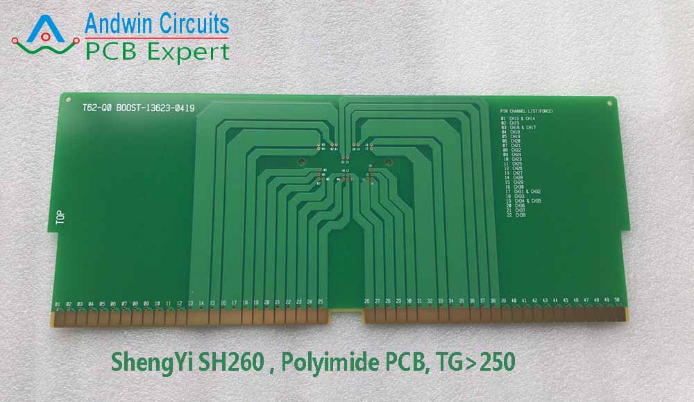
Hard gold (electrolytic gold) plating provides 30-50 micro-inch thickness with high durability for connector edge fingers. It withstands thousands of insertion/removal cycles in test sockets and ATE equipment without wear, maintaining reliable electrical contact.
Can you manufacture test boards with high Tg materials?
Yes, we use high Tg laminates including polyimide (Tg >250°C), ISOLA IS410, Shengyi SH260, and Rogers materials. High Tg materials maintain dimensional stability and electrical properties during high-temperature testing and thermal cycling.
What impedance control accuracy do you provide for IC test boards?
We achieve controlled impedance accuracy within ±5% (±10% standard) for single-ended and differential pairs. We provide impedance test reports with TDR (Time Domain Reflectometry) measurements for critical test board applications.
Do you support HDI technology for fine pitch IC testing?
Yes, we manufacture HDI PCBs with microvias, via-in-pad, blind and buried vias, and fine line capabilities down to 3/3 mil trace/space. HDI technology enables high-density routing for BGA packages and fine pitch IC connections.
What is the lead time for IC test board prototypes?
Standard prototype lead time is 5-10 days depending on layer count and complexity. We offer 24-72 hour expedited service for urgent test board development. High layer count boards (24-36 layers) typically require 10-15 days.
Get Started with Your IC Test Board Project
Ready to discuss your IC test board PCB requirements? Our engineering team can help optimize your design for signal integrity, impedance control, and test reliability.