
HDI PCB Manufacturing – High Density Interconnect PCB
Advanced 7+N+7 Capability | Laser Micro Vias 0.1mm | Up to 36 Layers | Fast Turnaround
What is HDI PCB
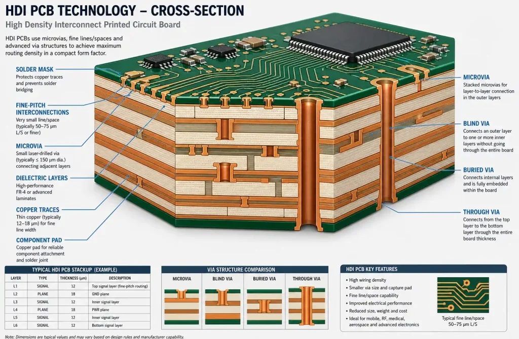
HDI PCB (High Density Interconnect PCB) uses advanced manufacturing technologies including laser-drilled micro vias, fine line traces, and high-density component placement to achieve superior circuit density in smaller form factors.
Our HDI PCB manufacturing capabilities include:
Core Capabilities
Complex HDI
stackup capability
Micro via technology
Any layer HDI capability
Medical/Military/Aerospace
Fine pitch support
HDI PCB Technical Specifications & Capabilities
| Specification | Standard Capability | Advanced Capability |
|---|---|---|
| Max Layers | 20 layers | 36 layers |
| HDI Structure | 1-2 step HDI (1+N+1, 2+N+2) | 3-4 step HDI, Any layer HDI (ELIC) |
| Laser Via Size | 0.15mm (6mil) | 0.1mm (4mil) |
| Min Track/Space | 4/4mil (0.1mm) | 3/3mil (0.075mm) |
| BGA Pitch | 0.4mm | 0.18mm |
| Build-up Layers | 1+N+1 to 3+N+3 | Up to 7+N+7 |
| Micro Via Type | Blind via, buried via | Stacked via, staggered via, copper filled |
| Board Thickness | 0.4mm – 3.2mm | 0.2mm – 6.0mm |
| Material Options | FR-4, High-Tg FR-4 | ITEQ, ShengYing, Rogers, PTFE |
| Surface Finish | HASL, ENIG | ENIG, Immersion Silver, OSP, ENEPIG |
| Min. Annular Ring | 3mil (0.075mm) | 2mil (0.05mm) |
| Turnaround Time | 10-15 days | 5-7 days (express) |
Need custom specifications? Our engineering team can handle special requirements. Contact Engineering Team
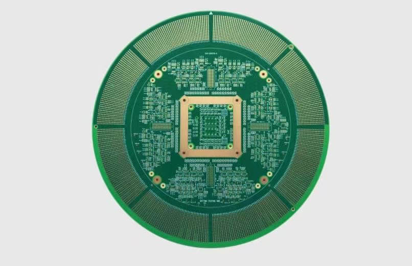
Key Features
Technical Features:
Performance Improvements:
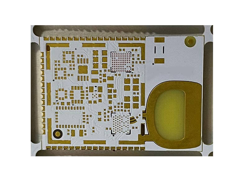
Benefits of HDI PCB
The transfer of heat is reduced due to close placement of components. Thermal expansion in HDI PCB endures less stress and extends endurance.
Vias in HDI PCB can be filled with conductive or non-conductive materials. Can facilitate transmission among components and customize according to board design.
Blind vias and via-in-pad enable components to be placed closely. Increases signal strength while transmission range and delay become less.
Better for saving space. Number of layers can be reduced without compromising efficiency and durability as well as the design of the application device.
HDI boards contain thinner lines, tighter spacing, and tighter annular ring using thinner specialty materials. Requires right amount of time, investment, and manufacturing process.
More efficient interconnections for highly complex large-pin count devices (such as CPU and GPU chips) to improve portable devices.
Stack up of HDI PCB
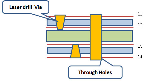
Stack up of 1 Step HDI PCB
the most like common PCB board,
after lamination ,laser drill out layer to sub out layer.
Stack up of 2 step HDI PCB
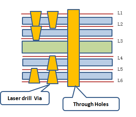
for example,a 6 Layers HDI PCB ,
first time, laminate L2 to L4 layer board ,
then laser drill L2-L3 or/and L4-L5,
and then finish other process.
HDI PCB stack up 6 layers 2 steps
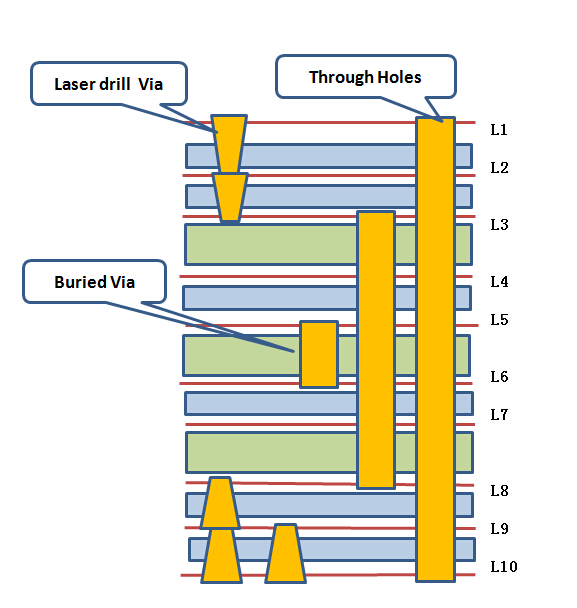
Stack up of 3 steps HDI with blind via and buried via
only differenci is that need more times lamination.
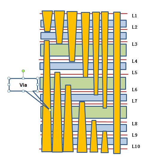
Anylayer connect of HDI PCB
but do not affect the orignal eletronical connect.
it is complex , depend on the orignal design of PCB.
Applications of HDI PCB
Medical
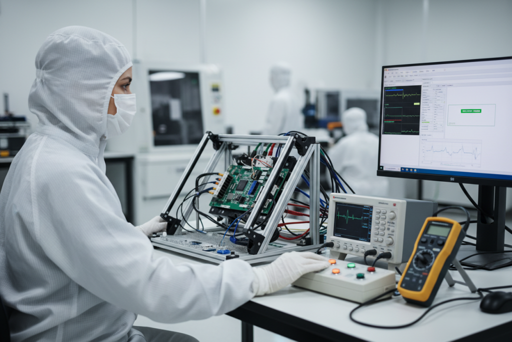
HDI PCBs enable compact, high-performance medical devices with reliable signal transmission. They are widely used in imaging systems, patient monitors, diagnostic equipment, implants, and portable medical electronics.
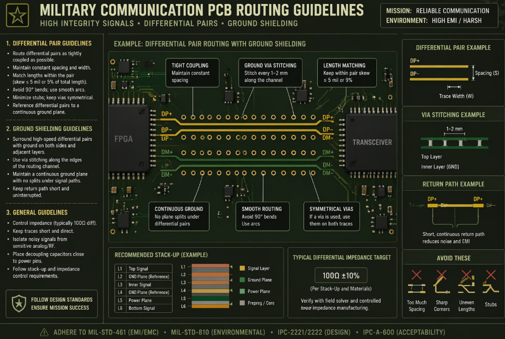
Military
Designed for demanding defense applications, HDI PCBs provide high reliability, compact layouts, and stable performance for military communication systems, radar equipment, and mission-critical electronics.
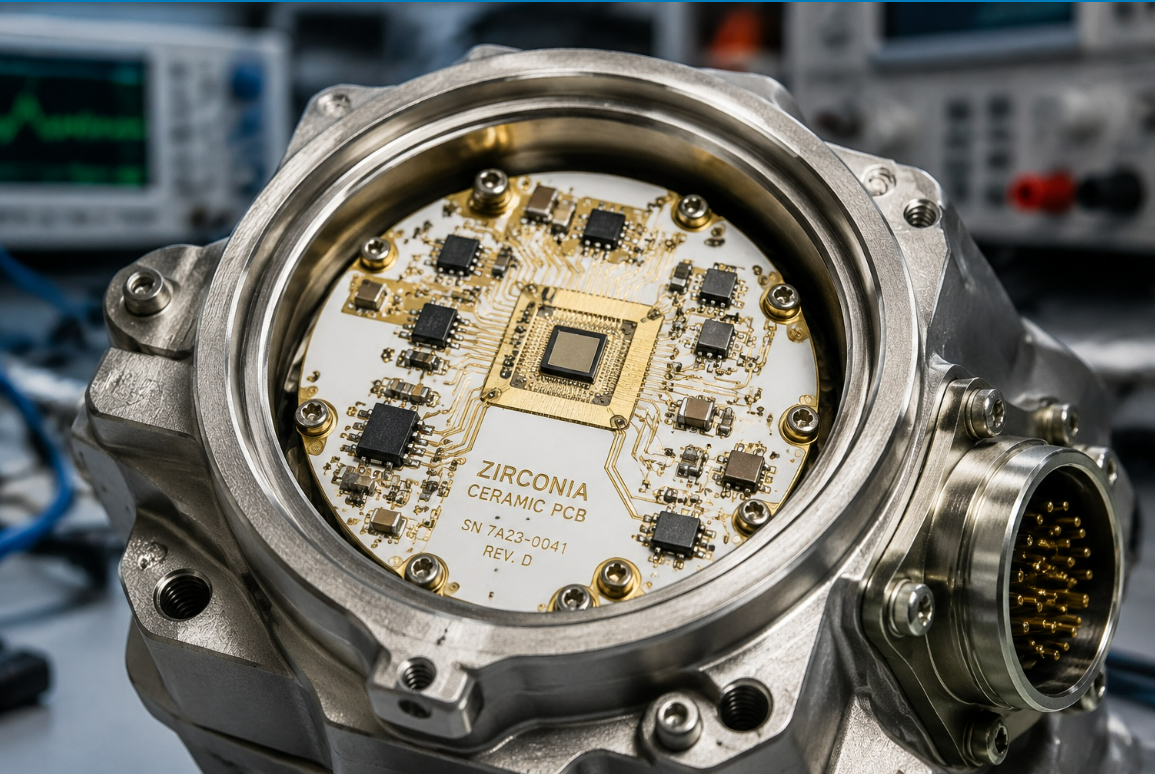
Aerospace
HDI PCBs deliver excellent durability and signal integrity in harsh environments. They are commonly used in avionics, navigation systems, satellites, and aerospace control equipment.
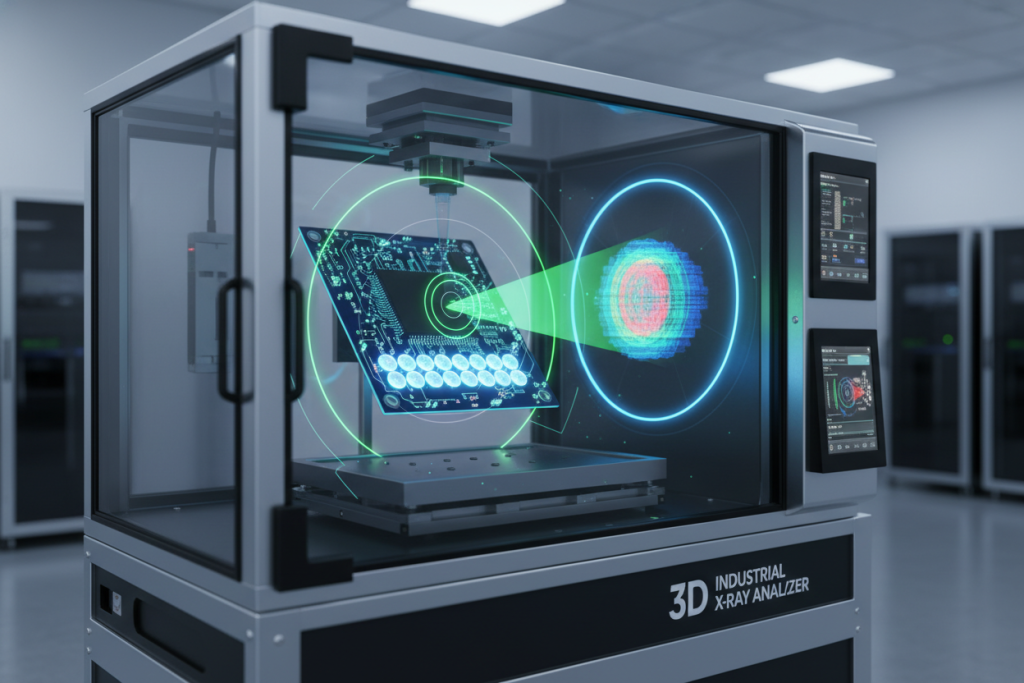
Automotive
HDI PCBs support advanced automotive electronics by reducing board size while improving performance. Typical applications include ADAS, infotainment systems, GPS, sensors, cameras, and electric vehicle control units.
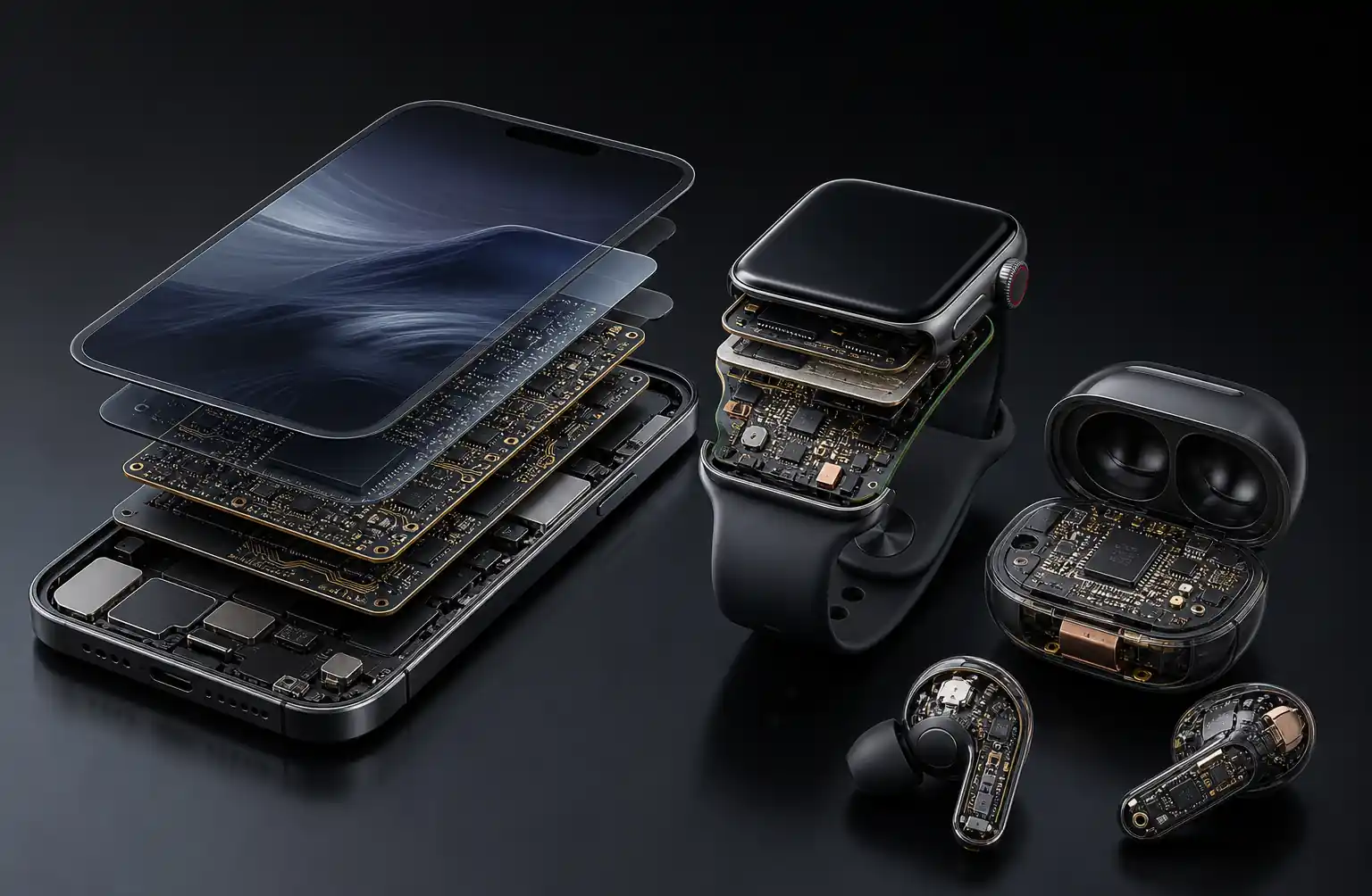
Consumer Electronics
HDI PCBs are ideal for compact electronic devices requiring high-speed signal transmission. They are widely used in smartphones, tablets, laptops, wearable devices, cameras, and IoT products.
HDI PCB vs Standard PCB Comparison
| Specification | Standard Capability | Advanced Capability |
|---|---|---|
| Max Layers | 20 layers | 36 layers |
| HDI Structure | 1-2 step HDI (1+N+1, 2+N+2) | 3-4 step HDI, Any layer HDI (ELIC) |
| Laser Via Size | 0.15mm (6mil) | 0.1mm (4mil) |
| Min Track/Space | 4/4mil (0.1mm) | 3/3mil (0.075mm) |
| BGA Pitch | 0.4mm | 0.18mm |
| Build-up Layers | 1+N+1 to 3+N+3 | Up to 7+N+7 |
| Micro Via Type | Blind via, buried via | Stacked via, staggered via, copper filled |
| Board Thickness | 0.4mm – 3.2mm | 0.2mm – 6.0mm |
| Material Options | FR-4, High-Tg FR-4 | ITEQ, ShengYing, Rogers, PTFE |
| Surface Finish | HASL, ENIG | ENIG, Immersion Silver, OSP, ENEPIG |
| Min. Annular Ring | 3mil (0.075mm) | 2mil (0.05mm) |
| Turnaround Time | 10-15 days | 5-7 days (express) |
Frequently Asked Questions
What is the difference between HDI PCB and standard PCB?
HDI PCBs use laser-drilled micro vias (0.1mm) and multiple build-up layers, while standard PCBs use mechanical drilled through-holes (0.3-0.5mm). This difference allows HDI PCBs to achieve 30-50% smaller board size, higher component density, better signal integrity, and support for fine-pitch BGAs (0.18mm vs 0.4mm).
What is the minimum via size for HDI PCB?
Andwin offers laser-drilled micro vias down to 0.1mm (4mil) diameter, enabling smaller pad area, higher routing density, and more compact designs compared to traditional PCB technology.
What HDI structure do I need?
The right HDI structure depends on your application complexity. 1-Step (1+N+1) is basic HDI and cost-effective for 6-10 layers. 2-Step (2+N+2) provides high density with fine-pitch BGA support for 8-16 layers. Any-Layer (ELIC) offers maximum design flexibility for complex routing in 10-24 layers. Contact our engineering team for DFM analysis of your specific design.
How long is the turnaround time?
Standard delivery for HDI PCB is 10-15 days, with express options available in 5-7 days. Actual turnaround depends on layer count and complexity, file readiness, and current production schedule. Submit your files for an accurate quote.
What materials are available?
We support standard materials including FR-4 and High-Tg FR-4, as well as specialty materials like ITEQ, ShengYing, Rogers, and PTFE. Material selection depends on your specific application requirements including frequency, temperature range, and performance characteristics.
What file formats do you accept?
We accept all standard PCB design formats including Gerber files (.gbr, .gbl), Excellon drill files (.xln), ODB++ format, and NC drill files. Submit your files via our contact form for an instant quote and free DFM analysis.
Ready to get your HDI PCB quoted?
Our engineering team provides free DFM analysis and design support.