
Copper Inlay PCB Manufacturing
Excellent thermal-management solution | Heat released through copper inlays to a bottom-side heatsink
Types Copper Inlay Capability
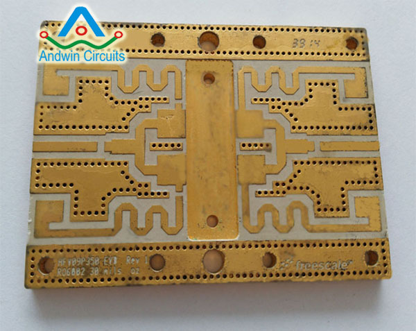
Copper inlay PCB is an excellent thermal-management solution: it releases heat from heater electronic components mounted on the PCB through copper inlays to a bottom-side heatsink.
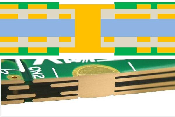
Bottom-Side Heatsink Path
Heat from heater components is released through copper inlays straight to a bottom-side heatsink — the most direct thermal route.
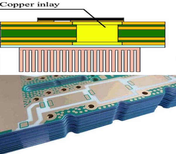
Components on Plated Via
Components can be mounted on the upper part of the through-hole by plating that part, integrating the heat source with the inlay.
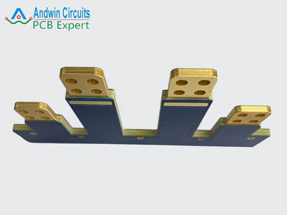
Copper Under Heat Source
Andwin presses copper into the board right under heat-generating components for efficient, localized heat dissipation.
Copper Inlay PCB — How It Works
The copper is pressed into the board right under the heat-generating component, and heat is carried through the inlay to the bottom heatsink. Key mechanism points:
Copper under hot spot
Copper is pressed into the board directly beneath the heat-generating component for the shortest thermal path.
To bottom heatsink
Heat is released through the copper inlays to a bottom-side heatsink — far more effective than relying on traces alone.
Plated through-hole mount
Components can be mounted on the upper part of the through-hole by plating that part, tying the source to the inlay.
Miniaturization ready
As parts shrink, natural dissipation drops; the inlay lets heat escape through the board instead of the part itself.
Why Choose Us?
20+ years experience — Andwin Circuits, PCB & PCBA manufacturer since 2003 (site copyright 2003–2026).
Efficient copper-inlay cooling — Copper inlay releases heater-component heat straight to a bottom-side heatsink, an excellent thermal-management solution.
Copper under the heat source — We press copper into the board right under heat-generating components for localized, efficient dissipation.
Plated through-hole mounting — Components can be mounted on the upper part of the plated through-hole, integrating source and inlay.
One-stop PCB + assembly — PCB fabrication and PCBA from one source; send Gerber + BOM to sales@andwinpcb.com for a quote.
Full certification — ISO 9001, IATF 16949, UL recognized and RoHS compliant processes.
Applications
Copper Inlay PCB is widely used across industries — especially in automotive parts that are critical to human safety.
LED lamp
Thermal-critical lighting where board-level heat transfer matters.
Inverter
Power stages with concentrated heat needing fast removal.
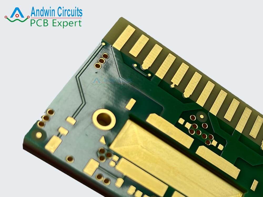
Electric Motorcycle
On-board power electronics under tight thermal budgets.
HighAutomotive (EV, HEV etc.)
Human-safety parts where reliable cooling is mandatory.
Frequently Asked Questions
1. What is a copper inlay PCB?
A copper inlay PCB embeds a solid piece of high-conductivity copper into the board right under the heat-generating component. The copper inlay carries heat to a bottom-side heatsink — an excellent thermal-management solution for high-power designs.
2. How does copper inlay dissipate heat?
The copper is pressed into the board directly beneath the hot component, so heat is released through the inlays to a bottom-side heatsink. This is far more effective than letting heat travel only through copper traces.
3. Can components be mounted on the inlay area?
Yes. Components can be mounted on the upper part of the through-hole by plating that part, tying the heat source directly to the copper inlay for better conduction.
4. Why is copper inlay good for miniaturized devices?
As parts shrink, natural heat dissipation from the component itself becomes difficult. The inlay lets heat escape through the PCB instead, so performance and life are maintained in compact layouts.
5. What is the lead time and minimum order quantity (MOQ)?
Lead time and MOQ depend on inlay shape, layer count, copper thickness and order volume. Send your Gerber, stack-up and thermal requirements to our sales team for an exact quote and schedule — we support prototypes and volume production.
Other PCB products, you may interesting


Get professional one stop PCB solution from us!
Our engineering team provides free DFM analysis and design support.