IoT and Wireless Communication PCBs
The Internet of Things (IoT) has transformed how we interact with technology. From smart home devices to industrial sensors, IoT applications rely on wireless connectivity to communicate and respond in real-time. According to recent statistics, 79% of US households now have at least one internet-connected device.
Andwin Circuits specializes in manufacturing PCBs for IoT and wireless communication applications since 2003. We deliver high-frequency, impedance-controlled, and compact circuit board solutions for 5G base stations, IoT endpoints, and wireless modules.
IoT and Wireless PCB Solutions
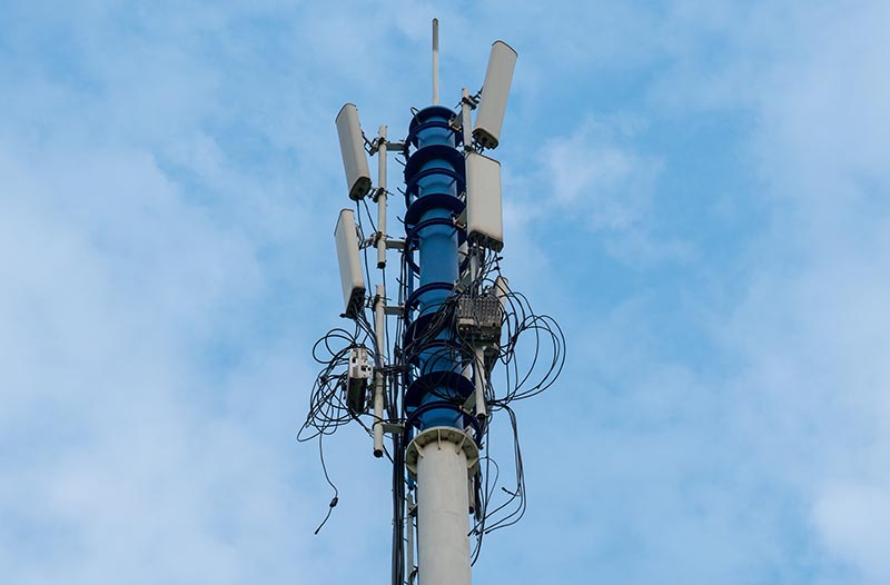
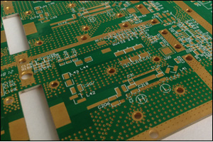
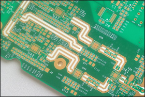
1. 5G Base Station / IoT Gateway
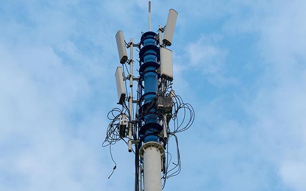
5G base stations provide wireless coverage and enable signal transmission between wired networks and wireless terminals. The architecture and design of base station PCBs directly impact 5G network deployment efficiency.
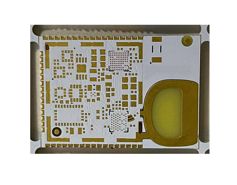
2. IoT Application End
IoT connections span across industries and permeate homes, offices, and vehicles. Applications include IBeacon positioning, smart logistics tracking, and intelligent sockets and switches.
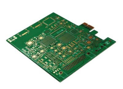
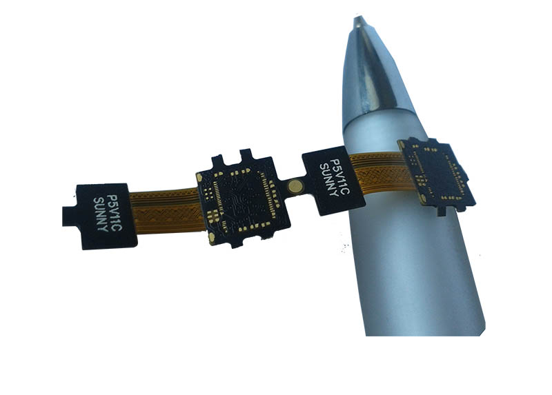


3. IoT Modules / Wifi / NB / LoRa / ZigBee
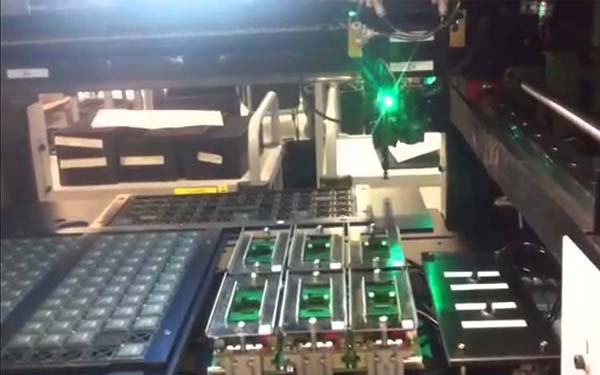
Wireless RF communication capability is critical for IoT device modules. These modules enable global connectivity for business, social media, e-commerce, and home automation applications.
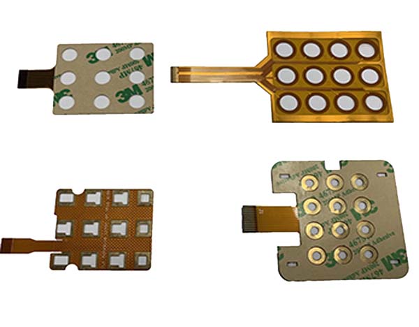
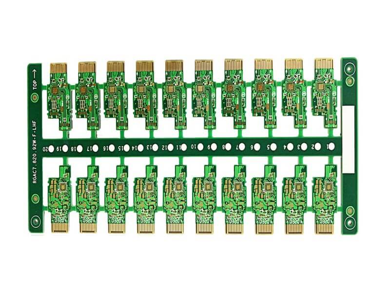
Why Choose Andwin Circuits
Manufacturing IoT and wireless PCBs since 2003 for smart devices and communication equipment worldwide.
Rogers, Megtron, and high-frequency laminates for optimal RF performance and signal integrity.
±5% impedance control, 1-20+ layers, HDI and rigid-flex capabilities, 3/3 mil trace/space.
24-72 hour prototypes, 5-7 day production. ISO 9001:2015, IPC-6012 Class 3, RoHS/REACH compliant.
Frequently Asked Questions
What PCB materials are best for IoT wireless applications?
For IoT devices operating below 6 GHz, Rogers 4350B or Megtron 6 provide excellent performance with cost efficiency. For higher frequency applications like 5G mmWave, Rogers 5880 is recommended for its low loss characteristics and stable dielectric properties.
How do you ensure impedance control for RF circuits in IoT devices?
We use controlled impedance manufacturing processes with precise dielectric thickness control and TDR (time-domain reflectometry) testing to verify impedance within ±5% tolerance, ensuring optimal signal transmission for wireless communication.
Can you manufacture compact PCBs for small IoT devices?
Yes, our HDI and rigid-flex PCB capabilities enable miniaturized designs with 0.1mm microvias, fine-pitch BGAs, and sequential lamination. We support compact form factors required for wearables, sensors, and portable IoT devices.
What is the lead time for IoT PCB prototypes?
Standard lead time is 5-7 days. We offer 24-72 hour expedited service for urgent IoT prototypes and development boards.
Do you support high-volume production for IoT devices?
Yes, we scale from prototypes to high-volume production with capacity up to 100,000+ pieces. We maintain consistent quality and competitive pricing for volume IoT projects.
What certifications do your IoT PCBs have?
Our PCBs are manufactured to ISO 9001:2015 and IPC-6012 Class 3 standards. All products are RoHS and REACH compliant, suitable for global IoT device deployment.
Get Started with Your IoT PCB Project
Ready to discuss your IoT and wireless communication PCB requirements? Our engineering team can help optimize your design for performance, size, and cost.