Skip to content
Andwin Circuits
  • Home
  • ProductsExpand
    • HDI multilayer PCB
    • Rigid Flex PCB
    • Flex pcb
    • Special PCBExpand
      • High Frequency PCBExpand
        • Rogers RO4350B PCB
        • Rogers RO4003 pcb
        • Rogers RO3003 PCB
        • Rogers 5880 PCB
        • DICLAD 527 PCB
        • Taconic TLX series
        • Taconic TLX-8 RF PCB
        • Taconic TLX-9 RF PCB
      • High speed pcbExpand
        • Megtron 6 High Speed PCB
        • TU-872 SLK Sp High Speed
      • High TG PCBExpand
        • SHENGYI SH260 PCB
        • ISOLA 370HR PCB
        • ISOLA IS410 PCB
        • ISOLA IS420 PCB
      • Heavy copper PCB
      • Copper coin pcb
      • Copper inlay PCB
    • Metal Core PCBExpand
      • Copper core pcb
      • Aluminum PCB
      • 2 Layers Aluminum PCB
      • Direct thermal MCPCB
      • 2 Layers Direct Thermal
    • Ceramic PCBExpand
      • DPC ceramic PCB
      • DBC ceramic PCB
      • Thick film Ceramic PCB
      • Al2O3 Alumina PCB
      • AIN ALN ceramic PCB
      • IGBT Ceramic PCB
  • ServiceExpand
    • PCB Assembly
    • Quick turn PCB assembly
    • PCBA conformal coating
  • IndustryExpand
    • Telecommunication
    • IoT and Wireless
    • Industrial Control
    • Thermal management
    • Power and Energy
    • IC test board
    • Automative
    • Medical
  • CapabilityExpand
    • Rigid PCB
    • Rigid flex PCB
    • Metal core PCB
    • PCB Assembly
  • TechnologyExpand
    • Blogs
    • Via in pad
    • PCB E-test
    • PCB stack up
    • MCPCB panelization
    • Controlled impedance PCB
  • AboutExpand
    • About us
    • Certification
    • Factory Tour
  • Contact
Andwin Circuits

What is  HDI PCBs?

High density interconnect (HDI) PCBs represent one of the fastest-growing segments of the printed circuit board market. Because of its higher circuitry density, the HDI PCB design can incorporate finer lines and spaces, smaller vias and capture pads, and higher connection pad densities. A high-density PCB features blind and buried vias and often contains microvias that are .006 in diameter or even less.

1.Multi-step HDI enables the connection between any layers;

2.Cross-layer laser processing can enhance the quality level of multi-step HDI;

3.The combination of HDI and high-frequency materials, metal-based laminates, FPC and other special laminates and processes enable the needs of high density and high frequency, high heat conducting, or 3D assembly.

Contact us for PCB quote now |

 HDI PCB Builds: 1+N+1, 2+N+2, 3+N+3, 4+N+4, 5+N+5

HDI builds means how many times of laser drilling for microvias. 1+N+1 is the simplest HDI build, and it means the HDI PCB’s microvias are single vias that need only one laser drilling.

Note

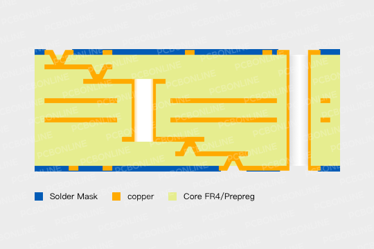
Microvias are drilled by laser (CO2 or UV) and penetrate only one PCB layer.

HDI PCB 2+N+2

2+N+2 means the HDI PCB needs twice laser drilling, and both the upper and bottom outer layers have 2 PCB layers. Unlike 1+N+1, 2+N+2 has two cases. One is that the microvias of the two adjacent outer layers overlap, and the two microvia form a stacked via. The other case is that the microvias of the two adjacent outer layers do not overlap, and they form a staggered via. As we know, it requires extremely high precision to locate and pile up two microvias, so stacked via HDI PCBs are more expensive than staggered via HID PCBs.

HDI builds

3+N+3 means the HDI PCBs need three times of laser drilling and both the upper and bottom outer layers have 3 PCB layers. And so on. The more times laser drilling, the higher the requirements for HDI PCB manufacturing technologies and more costs. 1+N+1, 2+N+2, 3+N+3, and 4+N+4 HDI PCBs are used commonly. 5+N+5 HDI PCBs are also in use but less. For example, the iPhone 6 uses the 5+N+5 HDI PCB as its mainboard.

Contact us for PCB quote now |

Address

Andwin Circuits Co.,Limited
Email: sales@andwinpcb.com
Tel: +86 755 2832 9394
Fax:+86 755 2992  6717
ADD:1-2F-1217,HouDeQun Industrial park,
NanTing RD NO.56,ShaJing,BaoAn,Shenzhen 518104,GuangDong,China

Products

  • HDI Multilayer PCB
  • Rigid Flex PCB
  • Flex pcb
  • High Frequency PCB
  • High speed pcb
  • Heavy copper PCB
  • Metal Core PCB
  • Ceramic PCB

Technology

  • Blogs
  • Via in pad
  • PCB E-test
  • PCB stack up
  • Metal core PCB panelization
  • Controlled impedance PCB

CERTIFICATION

Certification >>


Copyright© 2003 - 2026 Andwin | All Rights Reserved | Powered by Andwin

Scroll to top
  • Home
  • Products
    • HDI multilayer PCB
    • Rigid Flex PCB
    • Flex pcb
    • Special PCB
      • High Frequency PCB
        • Rogers RO4350B PCB
        • Rogers RO4003 pcb
        • Rogers RO3003 PCB
        • Rogers 5880 PCB
        • DICLAD 527 PCB
        • Taconic TLX series
        • Taconic TLX-8 RF PCB
        • Taconic TLX-9 RF PCB
      • High speed pcb
        • Megtron 6 High Speed PCB
        • TU-872 SLK Sp High Speed
      • High TG PCB
        • SHENGYI SH260 PCB
        • ISOLA 370HR PCB
        • ISOLA IS410 PCB
        • ISOLA IS420 PCB
      • Heavy copper PCB
      • Copper coin pcb
      • Copper inlay PCB
    • Metal Core PCB
      • Copper core pcb
      • Aluminum PCB
      • 2 Layers Aluminum PCB
      • Direct thermal MCPCB
      • 2 Layers Direct Thermal
    • Ceramic PCB
      • DPC ceramic PCB
      • DBC ceramic PCB
      • Thick film Ceramic PCB
      • Al2O3 Alumina PCB
      • AIN ALN ceramic PCB
      • IGBT Ceramic PCB
  • Service
    • PCB Assembly
    • Quick turn PCB assembly
    • PCBA conformal coating
  • Industry
    • Telecommunication
    • IoT and Wireless
    • Industrial Control
    • Thermal management
    • Power and Energy
    • IC test board
    • Automative
    • Medical
  • Capability
    • Rigid PCB
    • Rigid flex PCB
    • Metal core PCB
    • PCB Assembly
  • Technology
    • Blogs
    • Via in pad
    • PCB E-test
    • PCB stack up
    • MCPCB panelization
    • Controlled impedance PCB
  • About
    • About us
    • Certification
    • Factory Tour
  • Contact
Search