Skip to content
Andwin Circuits
  • Home
  • ProductsExpand
    • HDI multilayer PCB
    • Rigid Flex PCB
    • Flex pcb
    • Special PCBExpand
      • High Frequency PCBExpand
        • Rogers RO4350B PCB
        • Rogers RO4003 pcb
        • Rogers RO3003 PCB
        • Rogers 5880 PCB
        • DICLAD 527 PCB
        • Taconic TLX series
        • Taconic TLX-8 RF PCB
        • Taconic TLX-9 RF PCB
      • High speed pcbExpand
        • Megtron 6 High Speed PCB
        • TU-872 SLK Sp High Speed
      • High TG PCBExpand
        • SHENGYI SH260 PCB
        • ISOLA 370HR PCB
        • ISOLA IS410 PCB
        • ISOLA IS420 PCB
      • Heavy copper PCB
      • Copper coin pcb
      • Copper inlay PCB
    • Metal Core PCBExpand
      • Copper core pcb
      • Aluminum PCB
      • 2 Layers Aluminum PCB
      • Direct thermal MCPCB
      • 2 Layers Direct Thermal
    • Ceramic PCBExpand
      • DPC ceramic PCB
      • DBC ceramic PCB
      • Thick film Ceramic PCB
      • Al2O3 Alumina PCB
      • AIN ALN ceramic PCB
      • IGBT Ceramic PCB
  • ServiceExpand
    • PCB Assembly
    • Quick turn PCB assembly
    • PCBA conformal coating
  • IndustryExpand
    • Telecommunication
    • IoT and Wireless
    • Industrial Control
    • Thermal management
    • Power and Energy
    • IC test board
    • Automative
    • Medical
  • CapabilityExpand
    • Rigid PCB
    • Rigid flex PCB
    • Metal core PCB
    • PCB Assembly
  • TechnologyExpand
    • Blogs
    • Via in pad
    • PCB E-test
    • PCB stack up
    • MCPCB panelization
    • Controlled impedance PCB
  • AboutExpand
    • About us
    • Certification
    • Factory Tour
  • Contact
Andwin Circuits
Home / Blogs / Flex pcb design rules

Flex pcb design rules

ByGrace August 11, 2023June 14, 2024

When you begin to design your rigid flex PCB, there are a few rules you want to adhere to as best as possible:

  • Try not to bend at the corners. When making a bend, keep the bend curved rather than sharp.
  • Gradually change the width of the traces. Abruptly changing the trace width could result in a weak spot.
  • Try to keep the flex layers to a minimum of two for increased mechanical flexibility and reduced costs.

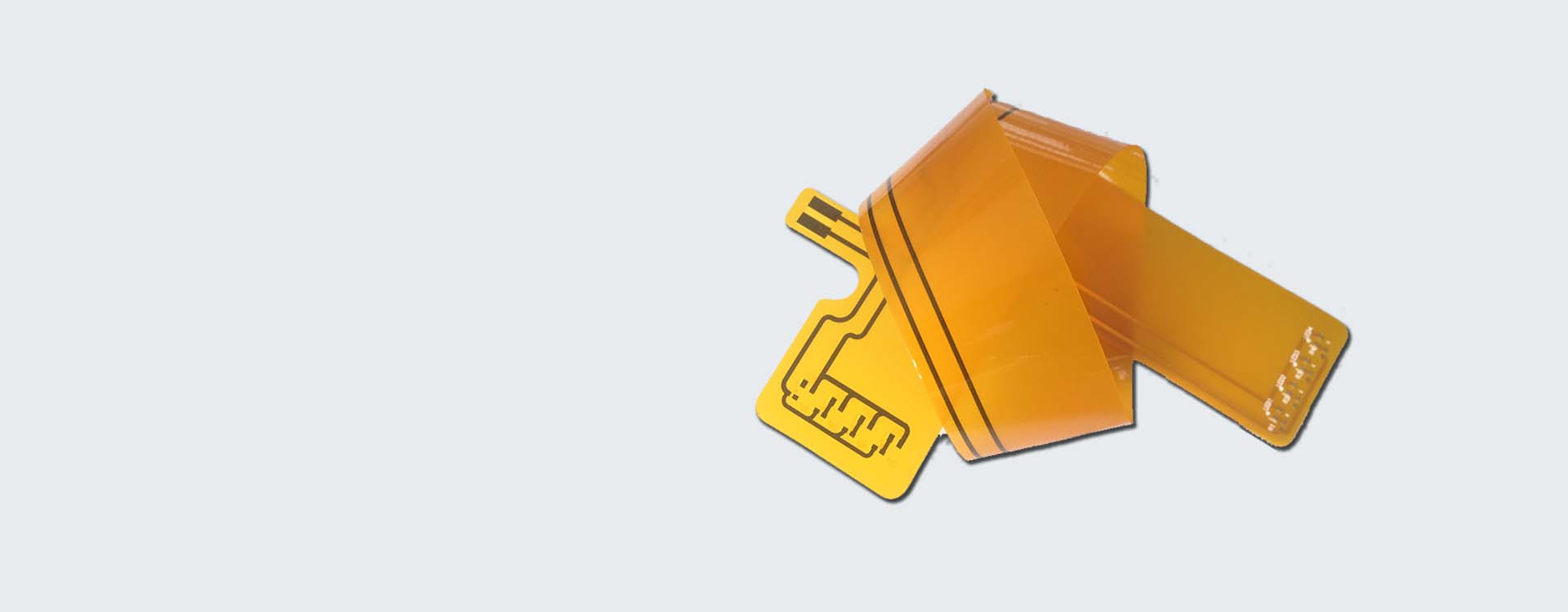
Pads and Vias on Flexible PCBs

The pads used for your rigid flex PCB should have anchoring spurs, also known as tie-downs.
The anchoring spurs help to ensure there is no separation between the base material and copper during the assembly.

The pads should also be filleted as to reduce the stress points, as well as the chance of breakage during flexing.

When calculating the pad size, it will depend on your board design and pad requirements specific to your application.
Use the following formula to calculate the pad size required:

Hole Size (finished) + Required Tolerances + All Flex Tolerance = Pad Size Required

Plated vias on the PCB are metalized through holes that connect the conductive layers on a flexible circuit.
There are also blind vias that connect the outer layer to the adjacent inner layer without going through the circuit.
Lastly, you also can use buried vias, which connect all the internal layers but do not connect the out layers.

The different via types can increase the space in the circuit to add component pads or more trace routing.

When it comes to using vias for the flex circuit, it is best to try and avoid them. However, if you must use them,
place the vias in areas where there will be no bends.

GET IN TOUCH!

1. Minimum trace width and spacing: The minimum trace width and spacing should be at least 0.1 mm.

2. Copper thickness: The copper thickness should be between 0.5 oz and 2 oz.

3. Pad size and shape: The pad size and shape should be designed to accommodate the component lead or connector pin.

4. Drill hole size: The minimum drill hole size should be 0.2 mm.

5. Annular ring: The annular ring should be at least 0.1 mm.

6. Solder mask: The solder mask should be designed to cover all exposed copper traces and pads.

7. Silkscreen: The silkscreen should be designed to provide clear and readable labeling of components and connectors.

8. Board outline: The board outline should be designed to fit the intended enclosure or mounting location.

9. Flexibility: The design should allow for the required flexibility of the flex PCB.

10. Stiffener placement: Stiffeners should be placed in areas where components or connectors are mounted to provide additional support.

flex pcb

Processing Guidelines for Flexible PCBs

You must dry your rigid flex PCB (roughly four hours at 120 degrees Celsius) to dry out any moisture absorbed by the polyimide.
After drying, you can then go through the placement and soldering process within eight hours.

GET IN TOUCH!

Post navigation

Previous Previous
Controlled impedance flex pcb
NextContinue
Flex pcb depaneling

Search

Search

Products

  • HDI Multilayer PCB
  • Rigid Flex PCB
  • Flex pcb
  • High Frequency PCB
  • High speed pcb
  • Heavy copper PCB
  • Metal Core PCB
  • Ceramic PCB

Address

Andwin Circuits Co.,Limited
Email: sales@andwinpcb.com
Tel: +86 755 2832 9394
Fax:+86 755 2992  6717
ADD:1-2F-1217,HouDeQun Industrial park,
NanTing RD NO.56,ShaJing,BaoAn,Shenzhen 518104,GuangDong,China

Products

  • HDI Multilayer PCB
  • Rigid Flex PCB
  • Flex pcb
  • High Frequency PCB
  • High speed pcb
  • Heavy copper PCB
  • Metal Core PCB
  • Ceramic PCB

Technology

  • Blogs
  • Via in pad
  • PCB E-test
  • PCB stack up
  • Metal core PCB panelization
  • Controlled impedance PCB

CERTIFICATION

Certification >>


Copyright© 2003 - 2026 Andwin | All Rights Reserved | Powered by Andwin

Scroll to top
  • Home
  • Products
    • HDI multilayer PCB
    • Rigid Flex PCB
    • Flex pcb
    • Special PCB
      • High Frequency PCB
        • Rogers RO4350B PCB
        • Rogers RO4003 pcb
        • Rogers RO3003 PCB
        • Rogers 5880 PCB
        • DICLAD 527 PCB
        • Taconic TLX series
        • Taconic TLX-8 RF PCB
        • Taconic TLX-9 RF PCB
      • High speed pcb
        • Megtron 6 High Speed PCB
        • TU-872 SLK Sp High Speed
      • High TG PCB
        • SHENGYI SH260 PCB
        • ISOLA 370HR PCB
        • ISOLA IS410 PCB
        • ISOLA IS420 PCB
      • Heavy copper PCB
      • Copper coin pcb
      • Copper inlay PCB
    • Metal Core PCB
      • Copper core pcb
      • Aluminum PCB
      • 2 Layers Aluminum PCB
      • Direct thermal MCPCB
      • 2 Layers Direct Thermal
    • Ceramic PCB
      • DPC ceramic PCB
      • DBC ceramic PCB
      • Thick film Ceramic PCB
      • Al2O3 Alumina PCB
      • AIN ALN ceramic PCB
      • IGBT Ceramic PCB
  • Service
    • PCB Assembly
    • Quick turn PCB assembly
    • PCBA conformal coating
  • Industry
    • Telecommunication
    • IoT and Wireless
    • Industrial Control
    • Thermal management
    • Power and Energy
    • IC test board
    • Automative
    • Medical
  • Capability
    • Rigid PCB
    • Rigid flex PCB
    • Metal core PCB
    • PCB Assembly
  • Technology
    • Blogs
    • Via in pad
    • PCB E-test
    • PCB stack up
    • MCPCB panelization
    • Controlled impedance PCB
  • About
    • About us
    • Certification
    • Factory Tour
  • Contact
Search