Skip to content
Andwin Circuits
  • Home
  • ProductsExpand
    • HDI multilayer PCB
    • Rigid Flex PCB
    • Flex pcb
    • Special PCBExpand
      • High Frequency PCBExpand
        • Rogers RO4350B PCB
        • Rogers RO4003 pcb
        • Rogers RO3003 PCB
        • Rogers 5880 PCB
        • DICLAD 527 PCB
        • Taconic TLX series
        • Taconic TLX-8 RF PCB
        • Taconic TLX-9 RF PCB
      • High speed pcbExpand
        • Megtron 6 High Speed PCB
        • TU-872 SLK Sp High Speed
      • High TG PCBExpand
        • SHENGYI SH260 PCB
        • ISOLA 370HR PCB
        • ISOLA IS410 PCB
        • ISOLA IS420 PCB
      • Heavy copper PCB
      • Copper coin pcb
      • Copper inlay PCB
    • Metal Core PCBExpand
      • Copper core pcb
      • Aluminum PCB
      • 2 Layers Aluminum PCB
      • Direct thermal MCPCB
      • 2 Layers Direct Thermal
    • Ceramic PCBExpand
      • DPC ceramic PCB
      • DBC ceramic PCB
      • Thick film Ceramic PCB
      • Al2O3 Alumina PCB
      • AIN ALN ceramic PCB
      • IGBT Ceramic PCB
  • ServiceExpand
    • PCB Assembly
    • Quick turn PCB assembly
    • PCBA conformal coating
  • IndustryExpand
    • Telecommunication
    • IoT and Wireless
    • Industrial Control
    • Thermal management
    • Power and Energy
    • IC test board
    • Automative
    • Medical
  • CapabilityExpand
    • Rigid PCB
    • Rigid flex PCB
    • Metal core PCB
    • PCB Assembly
  • TechnologyExpand
    • Blogs
    • Via in pad
    • PCB E-test
    • PCB stack up
    • MCPCB panelization
    • Controlled impedance PCB
  • AboutExpand
    • About us
    • Certification
    • Factory Tour
  • Contact
Andwin Circuits
Home / Blogs / blind via pcb

blind via pcb

ByGrace May 30, 2024June 12, 2024

1. What is a blind via PCB

Blind via PCB technology is a technology widely used in the design and manufacture of printed circuit boards (PCBs), and its main purpose is to achieve higher circuit density in a limited space.

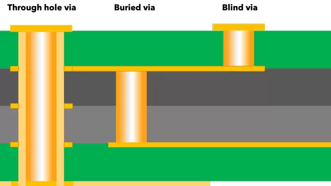
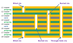
Blind vias refer to holes that extend from the surface layer of a PCB to the internal layer but do not penetrate the entire board.

This design enables the circuit board to achieve more complex circuit connections without increasing the number of layers, thereby improving the performance and functionality of the circuit board.

2. The principle of blind via PCB

The principle of blind via PCB is to establish an electrical connection between the surface layer and the internal layer of the PCB without penetrating the entire board.

This design not only saves space, but also reduces the path of signal transmission, thereby improving signal integrity and transmission speed. The manufacturing process of blind vias usually includes laser drilling and electroplating filling, which ensure the accuracy and reliability of blind vias.

GET PCB MANUFACTURING AND ASSEMBLY QUOTE NOW!

3. Application of blind via PCB technology

Blind via PCB technology is widely used in many fields.

First of all, in consumer electronics such as smartphones and tablets, blind via PCB technology enables smaller, lighter, and thinner designs while providing higher performance.

Secondly, in communication equipment, blind hole PCB technology helps to increase signal transmission speed and reduce signal interference, thereby improving the overall performance of the equipment. In addition, in automotive electronics and medical equipment, blind hole PCB technology is also widely used to meet the needs of high density and high reliability.

4. Advantages of blind hole PCB technology

The advantages of blind hole PCB technology are not only its ability to achieve higher circuit density and more complex circuit design, but also its ability to improve the performance and reliability of circuit boards.

First, the blind hole design reduces the path of signal transmission, thereby reducing signal delay and loss and improving signal integrity.

Secondly, the blind hole design reduces the number of layers of the circuit board, thereby reducing manufacturing costs and production time. In addition, the blind hole design is also able to improve the heat dissipation performance of the circuit board, thereby extending the service life of the equipment.

GET PCB AND ASSEMBLY SERVICE QUOTE NOW!

5. Challenges faced by blind hole PCB technology

However, there are also some challenges in blind hole PCB technology.

First, the manufacturing process of blind holes is relatively complex and requires high-precision equipment and technology, which increases the manufacturing cost.

Secondly, the design and manufacture of blind holes require a high degree of expertise and experience, which places higher requirements on designers and manufacturers.

In addition, the reliability and durability of blind holes also need to be rigorously tested and verified to ensure their stability and reliability in various applications.

In general, blind via PCB technology plays an important role in modern electronic devices. It improves the performance and functionality of devices by achieving higher circuit density and more complex circuit design in a limited space. Despite some challenges, the advantages of blind via PCB technology have made it widely used in many fields and promoted the continuous advancement of electronic technology.

GET PCB MANUFACTURING AND ASSEMBLY QUOTE NOW!

Post Tags: #blind via buried via#blind via in pcb#blind via pcb#pcb design#pcb via

Post navigation

Previous Previous
application of pcb design
NextContinue
How to design and make basic PCB circuits

Search

Search

Products

  • HDI Multilayer PCB
  • Rigid Flex PCB
  • Flex pcb
  • High Frequency PCB
  • High speed pcb
  • Heavy copper PCB
  • Metal Core PCB
  • Ceramic PCB

Address

Andwin Circuits Co.,Limited
Email: sales@andwinpcb.com
Tel: +86 755 2832 9394
Fax:+86 755 2992  6717
ADD:1-2F-1217,HouDeQun Industrial park,
NanTing RD NO.56,ShaJing,BaoAn,Shenzhen 518104,GuangDong,China

Products

  • HDI Multilayer PCB
  • Rigid Flex PCB
  • Flex pcb
  • High Frequency PCB
  • High speed pcb
  • Heavy copper PCB
  • Metal Core PCB
  • Ceramic PCB

Technology

  • Blogs
  • Via in pad
  • PCB E-test
  • PCB stack up
  • Metal core PCB panelization
  • Controlled impedance PCB

CERTIFICATION

Certification >>


Copyright© 2003 - 2026 Andwin | All Rights Reserved | Powered by Andwin

Scroll to top
  • Home
  • Products
    • HDI multilayer PCB
    • Rigid Flex PCB
    • Flex pcb
    • Special PCB
      • High Frequency PCB
        • Rogers RO4350B PCB
        • Rogers RO4003 pcb
        • Rogers RO3003 PCB
        • Rogers 5880 PCB
        • DICLAD 527 PCB
        • Taconic TLX series
        • Taconic TLX-8 RF PCB
        • Taconic TLX-9 RF PCB
      • High speed pcb
        • Megtron 6 High Speed PCB
        • TU-872 SLK Sp High Speed
      • High TG PCB
        • SHENGYI SH260 PCB
        • ISOLA 370HR PCB
        • ISOLA IS410 PCB
        • ISOLA IS420 PCB
      • Heavy copper PCB
      • Copper coin pcb
      • Copper inlay PCB
    • Metal Core PCB
      • Copper core pcb
      • Aluminum PCB
      • 2 Layers Aluminum PCB
      • Direct thermal MCPCB
      • 2 Layers Direct Thermal
    • Ceramic PCB
      • DPC ceramic PCB
      • DBC ceramic PCB
      • Thick film Ceramic PCB
      • Al2O3 Alumina PCB
      • AIN ALN ceramic PCB
      • IGBT Ceramic PCB
  • Service
    • PCB Assembly
    • Quick turn PCB assembly
    • PCBA conformal coating
  • Industry
    • Telecommunication
    • IoT and Wireless
    • Industrial Control
    • Thermal management
    • Power and Energy
    • IC test board
    • Automative
    • Medical
  • Capability
    • Rigid PCB
    • Rigid flex PCB
    • Metal core PCB
    • PCB Assembly
  • Technology
    • Blogs
    • Via in pad
    • PCB E-test
    • PCB stack up
    • MCPCB panelization
    • Controlled impedance PCB
  • About
    • About us
    • Certification
    • Factory Tour
  • Contact
Search