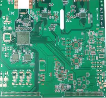
Skip to content
Andwin Circuits
  • Home
  • ProductsExpand
    • HDI multilayer PCB
    • Rigid Flex PCB
    • Flex pcb
    • Special PCBExpand
      • High Frequency PCBExpand
        • Rogers RO4350B PCB
        • Rogers RO4003 pcb
        • Rogers RO3003 PCB
        • Rogers 5880 PCB
        • DICLAD 527 PCB
        • Taconic TLX series
        • Taconic TLX-8 RF PCB
        • Taconic TLX-9 RF PCB
      • High speed pcbExpand
        • Megtron 6 High Speed PCB
        • TU-872 SLK Sp High Speed
      • High TG PCBExpand
        • SHENGYI SH260 PCB
        • ISOLA 370HR PCB
        • ISOLA IS410 PCB
        • ISOLA IS420 PCB
      • Heavy copper PCB
      • Copper coin pcb
      • Copper inlay PCB
    • Metal Core PCBExpand
      • Copper core pcb
      • Aluminum PCB
      • 2 Layers Aluminum PCB
      • Direct thermal MCPCB
      • 2 Layers Direct Thermal
    • Ceramic PCBExpand
      • DPC ceramic PCB
      • DBC ceramic PCB
      • Thick film Ceramic PCB
      • Al2O3 Alumina PCB
      • AIN ALN ceramic PCB
      • IGBT Ceramic PCB
  • ServiceExpand
    • PCB Assembly
    • Quick turn PCB assembly
    • PCBA conformal coating
  • IndustryExpand
    • Telecommunication
    • IoT and Wireless
    • Industrial Control
    • Thermal management
    • Power and Energy
    • IC test board
    • Automative
    • Medical
  • CapabilityExpand
    • Rigid PCB
    • Rigid flex PCB
    • Metal core PCB
    • PCB Assembly
  • TechnologyExpand
    • Blogs
    • Via in pad
    • PCB E-test
    • PCB stack up
    • MCPCB panelization
    • Controlled impedance PCB
  • AboutExpand
    • About us
    • Certification
    • Factory Tour
  • Contact
Andwin Circuits
Home / Blogs / custom pcb board

custom pcb board

ByGrace May 31, 2024June 11, 2024

custom pcb board

The design process of custom PCB boards is a complex and delicate process involving multiple steps and technical details. First, the starting point of the design process is demand analysis. In the demand analysis stage, engineers need to clarify the functions, dimensions, materials and other specific requirements of the circuit board. This step is crucial because it determines the direction and specific parameters of the subsequent design.

1. PCB board customization process

(1)Draw the circuit schematic

Next, enter the schematic design phase. In this phase, engineers use professional design software to draw the circuit schematic to ensure that all electronic components and connection relationships are accurate. Schematic design is not only the basis for circuit board design, but also provides necessary reference for subsequent PCB layout. Through the schematic, engineers can clearly understand the working principle of the circuit and the relationship between the various components.

(2)PCB layout design

After completing the schematic design, enter the PCB layout design phase. In this phase, engineers convert the schematic into an actual PCB layout. The layout design needs to consider factors such as the size of the circuit board, the placement of components, the routing path, and electromagnetic compatibility. In order to ensure the performance and reliability of the circuit board, engineers need to repeatedly adjust and optimize the layout to avoid signal interference and heat accumulation.

(3)Electrical rule check

After the layout design is completed, the electrical rule check (ERC) and design rule check (DRC) are performed. These two check steps are designed to discover and correct potential errors in the design. The ERC check focuses on the correctness of the electrical connection, while the DRC check focuses on the rationality of the physical layout. Through these two checks, engineers can ensure that the design meets the specifications and reduce problems in subsequent production.

(4)Component package and library management

Then, the component package and library management stage is entered. In this stage, engineers need to select the appropriate package for each electronic component and ensure that the information in the component library is accurate. The choice of component package directly affects the manufacturing and assembly of the PCB, so special care is required.

After completing the above steps, the production file generation stage is entered. The production files include Gerber files, drilling files, and assembly drawings, etc. These files are the basis for PCB manufacturers to produce. When generating production files, engineers need to ensure the integrity and accuracy of the files to avoid problems in the production process.

Finally, sample production and testing are carried out. In the sample production stage, the manufacturer produces samples based on the production files and conducts a series of tests to verify the correctness and performance of the design. After the test is passed, it will enter the mass production stage.

GET PCB MANUFACTURING AND ASSEMBLY QUOTE NOW!

GET PCB AND ASSEMBLY SERVICE QUOTE NOW!

In summary, the design process of custom PCB boards is a systematic and refined process, and each step is crucial. Through a rigorous design and inspection process, engineers can ensure that the final PCB board meets the expected functional and performance requirements.

the five key steps of custom PCB board design are interrelated and interlocking. Each step requires designers to have solid professional knowledge and rich practical experience. Only through a scientific and reasonable design process can the efficient operation and reliability of electronic products be ensured.

GET PCB MANUFACTURING AND ASSEMBLY QUOTE NOW!

Post Tags: #custom pcb board#pcb design

Post navigation

Previous Previous
copper circuit board
NextContinue
multilayer pcb

Search

Search

Products

  • HDI Multilayer PCB
  • Rigid Flex PCB
  • Flex pcb
  • High Frequency PCB
  • High speed pcb
  • Heavy copper PCB
  • Metal Core PCB
  • Ceramic PCB

Address

Andwin Circuits Co.,Limited
Email: sales@andwinpcb.com
Tel: +86 755 2832 9394
Fax:+86 755 2992  6717
ADD:1-2F-1217,HouDeQun Industrial park,
NanTing RD NO.56,ShaJing,BaoAn,Shenzhen 518104,GuangDong,China

Products

  • HDI Multilayer PCB
  • Rigid Flex PCB
  • Flex pcb
  • High Frequency PCB
  • High speed pcb
  • Heavy copper PCB
  • Metal Core PCB
  • Ceramic PCB

Technology

  • Blogs
  • Via in pad
  • PCB E-test
  • PCB stack up
  • Metal core PCB panelization
  • Controlled impedance PCB

CERTIFICATION

Certification >>


Copyright© 2003 - 2026 Andwin | All Rights Reserved | Powered by Andwin

Scroll to top
  • Home
  • Products
    • HDI multilayer PCB
    • Rigid Flex PCB
    • Flex pcb
    • Special PCB
      • High Frequency PCB
        • Rogers RO4350B PCB
        • Rogers RO4003 pcb
        • Rogers RO3003 PCB
        • Rogers 5880 PCB
        • DICLAD 527 PCB
        • Taconic TLX series
        • Taconic TLX-8 RF PCB
        • Taconic TLX-9 RF PCB
      • High speed pcb
        • Megtron 6 High Speed PCB
        • TU-872 SLK Sp High Speed
      • High TG PCB
        • SHENGYI SH260 PCB
        • ISOLA 370HR PCB
        • ISOLA IS410 PCB
        • ISOLA IS420 PCB
      • Heavy copper PCB
      • Copper coin pcb
      • Copper inlay PCB
    • Metal Core PCB
      • Copper core pcb
      • Aluminum PCB
      • 2 Layers Aluminum PCB
      • Direct thermal MCPCB
      • 2 Layers Direct Thermal
    • Ceramic PCB
      • DPC ceramic PCB
      • DBC ceramic PCB
      • Thick film Ceramic PCB
      • Al2O3 Alumina PCB
      • AIN ALN ceramic PCB
      • IGBT Ceramic PCB
  • Service
    • PCB Assembly
    • Quick turn PCB assembly
    • PCBA conformal coating
  • Industry
    • Telecommunication
    • IoT and Wireless
    • Industrial Control
    • Thermal management
    • Power and Energy
    • IC test board
    • Automative
    • Medical
  • Capability
    • Rigid PCB
    • Rigid flex PCB
    • Metal core PCB
    • PCB Assembly
  • Technology
    • Blogs
    • Via in pad
    • PCB E-test
    • PCB stack up
    • MCPCB panelization
    • Controlled impedance PCB
  • About
    • About us
    • Certification
    • Factory Tour
  • Contact
Search