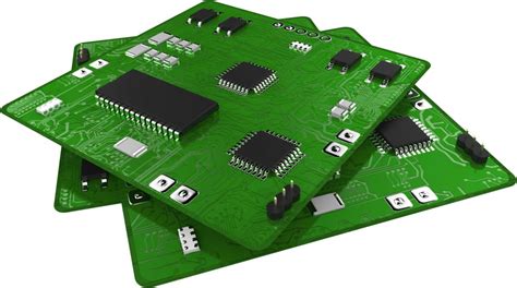
Design custom pcb
Essential Steps For Designing A Custom PCB
Designing a custom printed circuit board (PCB) is a meticulous process that requires careful planning and execution. The journey begins with a clear understanding of the project requirements, which involves defining the functionality, size, and shape of the PCB. This initial phase is crucial as it sets the foundation for the entire design process. Once the requirements are established, the next step is to create a schematic diagram. This diagram serves as a blueprint, illustrating how different components will be connected. It is essential to ensure that the schematic is accurate and comprehensive, as any errors at this stage can lead to significant issues later on.
Following the creation of the schematic, the next phase involves selecting the appropriate components.
This step requires a thorough understanding of the electrical and mechanical properties of each component. It is important to choose components that not only meet the functional requirements but also fit within the physical constraints of the PCB. Additionally, considering factors such as availability, cost, and reliability is crucial to avoid potential delays and budget overruns.
Once the components are selected, the layout design begins.
This involves placing the components on the PCB and routing the electrical connections between them. The layout design is a critical step that requires a balance between functionality and manufacturability. It is important to follow design rules and guidelines to ensure that the PCB can be manufactured without issues. For instance, maintaining adequate spacing between components and traces is essential to prevent short circuits and signal interference. Moreover, considering thermal management and signal integrity during the layout design can significantly enhance the performance and reliability of the PCB.
After completing the layout design, the next step is to perform a design rule check (DRC).
This automated process verifies that the design adheres to the specified rules and guidelines. It helps identify potential issues such as overlapping components, insufficient spacing, and incorrect trace widths. Addressing these issues at this stage can save time and resources by preventing costly revisions later in the process.
Following the DRC, it is advisable to conduct a thorough review of the design.
This review should involve multiple stakeholders, including engineers, designers, and project managers, to ensure that all aspects of the design have been considered. This collaborative approach can help identify potential issues that may have been overlooked and ensure that the design meets all requirements.
Once the design is reviewed and approved, the next step is to generate the necessary files for manufacturing.
These files typically include Gerber files, which contain the information needed to fabricate the PCB, and a bill of materials (BOM), which lists all the components required for assembly. It is important to ensure that these files are accurate and complete to avoid any issues during the manufacturing process.
Finally, the PCB is sent to a manufacturer for fabrication and assembly.
It is important to choose a reputable manufacturer with experience in producing custom PCBs to ensure high-quality results. Once the PCB is manufactured, it undergoes testing to verify that it functions as intended. This testing phase is crucial to identify any defects or issues that need to be addressed before the PCB can be deployed.
In conclusion, designing a custom PCB involves a series of essential steps, each requiring careful attention to detail. From defining the project requirements and creating a schematic diagram to selecting components, designing the layout, and conducting reviews, each step plays a vital role in ensuring the success of the final product. By following these steps diligently, designers can create custom PCBs that meet their specific needs and perform reliably in their intended applications.
Top Software Tools For Custom PCB Design
Designing custom printed circuit boards (PCBs) is a critical task in the development of electronic devices, requiring precision, expertise, and the right set of tools. The software tools available for PCB design have evolved significantly, offering a range of features that cater to both novice designers and seasoned professionals. Selecting the appropriate software can streamline the design process, enhance productivity, and ensure the final product meets all necessary specifications. In this article, we will explore some of the top software tools for custom PCB design, highlighting their unique features and benefits.
One of the most widely recognized tools in the PCB design industry is Altium Designer.
Known for its comprehensive suite of features, Altium Designer offers an integrated environment that combines schematic capture, PCB layout, and design rule checking. This software is particularly favored for its user-friendly interface and robust library management system, which allows designers to easily access and manage components. Additionally, Altium Designer supports advanced routing capabilities and 3D visualization, enabling designers to view their boards in a three-dimensional space and detect potential issues early in the design process.
Transitioning to another popular tool, Eagle by Autodesk stands out for its affordability and flexibility.
Eagle, which stands for Easily Applicable Graphical Layout Editor, is a powerful tool that provides a range of functionalities, including schematic capture, PCB layout, and auto-routing. One of Eagle’s key advantages is its extensive component library, which simplifies the process of finding and integrating components into the design. Moreover, Eagle’s user community is highly active, offering a wealth of tutorials, forums, and shared libraries that can be invaluable resources for both beginners and experienced designers.
Another noteworthy mention is KiCad, an open-source PCB design tool that has gained significant traction in recent years.
KiCad offers a full suite of design tools, including schematic capture, PCB layout, and a 3D viewer. One of the primary benefits of KiCad is its cost-effectiveness, as it is free to use without any licensing fees. Despite being open-source, KiCad does not compromise on functionality, providing a robust platform that supports complex designs and high levels of customization. Furthermore, KiCad’s active development community continuously contributes to its improvement, ensuring that it remains a competitive option in the PCB design landscape.
For those seeking a cloud-based solution, Upverter offers a unique approach to PCB design.
Upverter allows designers to work collaboratively in real-time, making it an excellent choice for teams spread across different locations. The platform includes features such as schematic capture, PCB layout, and version control, ensuring that all team members are working with the most up-to-date design files. Additionally, Upverter’s cloud-based nature eliminates the need for software installation and maintenance, providing a seamless and efficient design experience.
Lastly, DipTrace is another versatile tool that deserves mention.
DipTrace offers a range of features, including schematic capture, PCB layout, and 3D modeling. One of DipTrace’s standout features is its intuitive user interface, which simplifies the learning curve for new users. Additionally, DipTrace supports a variety of file formats, making it easy to import and export designs from other software tools. This flexibility, combined with its powerful design capabilities, makes DipTrace a valuable tool for both hobbyists and professional designers.
In conclusion, the choice of PCB design software can significantly impact the efficiency and success of your design projects. Whether you prioritize advanced features, cost-effectiveness, or collaborative capabilities, there is a tool available to meet your specific needs. By carefully evaluating the options and selecting the right software, you can enhance your design process and achieve high-quality results in your custom PCB projects.
Common Mistakes To Avoid In PCB Design
Designing custom printed circuit boards (PCBs) is a meticulous process that requires a blend of technical expertise and attention to detail. However, even seasoned designers can fall prey to common mistakes that can compromise the functionality and reliability of the final product. One of the most frequent errors is inadequate planning. Before diving into the design software, it is crucial to have a clear understanding of the project requirements, including the electrical specifications, mechanical constraints, and environmental conditions. Failing to do so can lead to a cascade of issues that are difficult to rectify later in the design process.
Another prevalent mistake is poor component placement.
The arrangement of components on a PCB is not merely a matter of fitting everything within the board’s dimensions. It involves strategic positioning to minimize signal interference, optimize thermal management, and ensure ease of assembly. For instance, placing high-speed components too close to each other can result in signal integrity problems, while poor thermal management can lead to overheating and reduced lifespan of the components. Therefore, it is essential to follow best practices for component placement, such as keeping analog and digital components separate and placing decoupling capacitors close to the power pins of integrated circuits.
In addition to component placement, improper routing of traces is another common pitfall.
The layout of the traces, which connect the various components, plays a critical role in the performance of the PCB. Sharp angles, inconsistent trace widths, and inadequate spacing between traces can all contribute to signal degradation and electromagnetic interference (EMI). To avoid these issues, designers should adhere to guidelines for trace routing, such as using 45-degree angles instead of 90-degree bends and maintaining consistent trace widths. Additionally, it is advisable to use ground planes and shielding techniques to mitigate EMI.
Moreover, neglecting to perform thorough design rule checks (DRCs) can lead to costly errors.
DRCs are automated checks that verify the design against a set of predefined rules, such as minimum trace width, spacing, and hole size. Skipping this step or not configuring the DRC settings correctly can result in a design that is not manufacturable or fails to meet the required standards. Therefore, it is imperative to run DRCs at various stages of the design process and address any violations promptly.
Another area where designers often falter is in the selection of materials and finishes.
The choice of substrate material, copper thickness, and surface finish can significantly impact the performance and durability of the PCB. For example, using a substrate with poor thermal conductivity can lead to overheating issues, while an inappropriate surface finish can result in poor solderability and increased risk of corrosion. Hence, it is important to select materials and finishes that are compatible with the intended application and operating environment.
Furthermore, inadequate documentation is a mistake that can cause significant delays and misunderstandings during the manufacturing and assembly stages.
Comprehensive documentation, including schematics, bill of materials (BOM), assembly drawings, and test procedures, is essential for ensuring that the PCB is built and tested correctly. Incomplete or unclear documentation can lead to errors, rework, and increased costs.
In conclusion, avoiding these common mistakes in PCB design requires a combination of careful planning, adherence to best practices, and thorough verification. By taking the time to plan the design, strategically place components, route traces correctly, perform DRCs, select appropriate materials, and provide detailed documentation, designers can create reliable and high-performance PCBs that meet the project’s requirements.
Innovative Trends In Custom PCB Design
In the rapidly evolving world of electronics, the design of custom printed circuit boards (PCBs) has become a cornerstone of innovation. As technology advances, so too do the methods and materials used in PCB design, leading to a host of innovative trends that are reshaping the industry.
One of the most significant trends is the miniaturization of components.
As devices become smaller and more powerful, the demand for compact, high-density PCBs has surged. This trend is driven by the need for portable electronics, such as smartphones and wearable devices, which require intricate designs to fit more functionality into less space. Consequently, designers are increasingly utilizing advanced techniques like microvia technology and high-density interconnects (HDI) to achieve these compact designs.
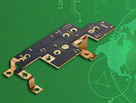
Another noteworthy trend is the integration of flexible and rigid-flex PCBs.
These types of PCBs offer a unique combination of flexibility and durability, making them ideal for applications where space constraints and mechanical stress are concerns. For instance, in medical devices and aerospace applications, the ability to bend and twist without compromising performance is crucial. This flexibility also allows for more creative and efficient use of space within a device, leading to more innovative product designs.
Moreover, the rise of the Internet of Things (IoT) has spurred the development of PCBs with enhanced connectivity features.
IoT devices require reliable and efficient communication capabilities, which has led to the incorporation of advanced wireless technologies such as Bluetooth, Wi-Fi, and NFC directly into the PCB design. This integration not only simplifies the overall design but also improves the performance and reliability of the device. Additionally, the use of embedded components, such as resistors and capacitors, within the PCB itself is becoming more prevalent. This approach reduces the need for external components, further streamlining the design and improving signal integrity.
Sustainability is also becoming a key consideration in custom PCB design.
As environmental concerns grow, there is a push towards using eco-friendly materials and manufacturing processes. Lead-free soldering, for example, is now a standard practice in many regions, reducing the environmental impact of electronic waste. Furthermore, designers are exploring the use of biodegradable substrates and other sustainable materials to create more environmentally friendly PCBs. This shift not only addresses regulatory requirements but also aligns with the growing consumer demand for greener products.
In addition to these material and design innovations, advancements in software tools are revolutionizing the PCB design process.
Modern design software offers powerful simulation and analysis capabilities, allowing designers to test and optimize their designs before physical prototyping. This not only speeds up the development process but also reduces costs and minimizes the risk of errors. Furthermore, the integration of artificial intelligence (AI) and machine learning (ML) into design tools is enabling more intelligent and automated design processes. These technologies can analyze vast amounts of data to suggest optimal design solutions, predict potential issues, and even automate routine tasks, freeing up designers to focus on more complex and creative aspects of their work.
As we look to the future, it is clear that the landscape of custom PCB design will continue to evolve, driven by technological advancements and changing market demands. The trends of miniaturization, flexible and rigid-flex PCBs, enhanced connectivity, sustainability, and advanced design tools are just the beginning. As designers push the boundaries of what is possible, we can expect to see even more innovative and sophisticated PCBs that will power the next generation of electronic devices.