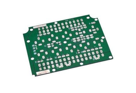
PCB circuit board layer full resolution
A. The bottom pad layer of the top layer of the PCB circuit board:
Toppaste and Bottompaste are the bottom pad layer of the top layer. It refers to the exposed copper we can see. (For example, we drew a wire in the top wiring layer. This wire we see on the PCB is just A line only, it is covered by the entire green oil, but we draw a square, or a point, on the toppaset layer on the position of this line. Oil, but copper platinum.
The two layers, topsolder and bottomsolder, are just opposite to the previous two layers.
It can be said that these two layers are the layers that cover the green oil. solder: paste: paste, paste mask: cover, film, surface layer, etc. Take the top layer as an example: 1.solder layer in the protel 99SE full name is top solder mask, which means that the solder mask, according to the literal meaning to understand is to pcb on the line of a layer of green oil, to achieve resistance The purpose of welding, in fact, is not, if you do not add the solder layer in the trace after the line, the green oil is produced by the pcb manufacturer when the default is to add, if the solder layer is added, pcb after being made, in this Will see the exposed copper foil. It can be understood as a mirror phase.
Second, the past layer is used when the stencil is made before the pcb patch. It is used to apply solder paste.
The electronic components of the patch are affixed to the solder paste for reflow. The difference between DrillGuide and DrillDrawing is:
1. DrillGuide is used to guide For drilling holes, the C8051 chip decrypts, which is mainly used for manual drilling to locate
2. DrillDrawing is used to view the drilling hole. When the manual drilling, the two files to be used in conjunction. However, most of them are digitally controlled boreholes, so the two layers are not very useful. When placing the positioning holes, it is not necessary to place the contents on these two layers, as long as the via hole of the corresponding aperture is placed on the bottom of the layer of Microwave or TOPLAYER or bottom layer, but the diameter of the disk can not be placed smaller.
The two layers of Michanical and MultiLayer are as follows:
1. Michanical is a mechanical layer for placing mechanical graphics, such as the shape of a PCB, etc.
2. MultiLayer can be called a multilayer, and the graphics placed on this layer are on any layer.
There is a corresponding pattern, and the keepout layer that will not be screen-printed with solder resist is not actually used for drawing PCB outlines. The real purpose of the keepout layer is to prohibit the wiring, that is, after placing the pattern on the keepout layer, Corresponding positions on the wiring layer (such as: toplayer and bottomlayer) do not appear to have corresponding graphic copper foils, and are all wiring layers. This does not happen when the graphics are placed on the Michanical layer.
Third, the mechanical layer is the definition of the appearance of the entire PCB board, in fact, when we say that the mechanical layer refers to the overall structure of the PCB board.
Disabling the wiring layer is the one-time boundary that defines the electrical characteristics of our cloth. That is to say, after we have defined the disabling of the wiring layer, it is impossible for us to exceed the prohibition of wiring during the subsequent cloth process. The boundaries of the layers.
Topoverlay and bottomoverlay are the silkscreen characters that define the top and bottom layers, which are the component numbers and some characters we normally see on the PCB. Toppaste and Bottompaste are the bottom pad layer of the top layer. It refers to the exposed copper we can see. (For example, we drew a wire in the top wiring layer.
This wire we see on the PCB is just A line only, it is covered by the entire green oil, but we draw a square, or a point, on the toppaset layer on the position of this line. It is oil, but copper and platinum.The two layers, topsolder and bottomsolder, are just opposite to the first two layers. It can be said that these two layers are the layers that cover the green oil, and the multilaye layer is almost the same as the mechanical layer. As the name implies, this layer refers to all layers of the PCB board.
1. The concept of “Layer” is similar to the concept of “layer” introduced in word processing or many other softwares for the nesting and synthesis of graphs, texts, colors, etc.
The “layer” of Protel is not virtual. Instead, the printed board material itself is real on each copper foil layer. Nowadays, components of electronic circuits are densely installed. With special requirements such as anti-interference and wiring, printed boards used in some newer electronic products not only have upper and lower sides for wiring, but also have interlayer copper foils that can be specially processed in the middle of the board, for example, now used by computer motherboards.
The printing plate material is more than 4 layers. These layers are mostly used for setting the power wiring layers (such as Ground Dever and Power Dever in software) that are relatively difficult to process because they are relatively difficult to process, and are often used for wiring with large area filling methods (such as ExternaI P1a11e and Fill in software). ).
The surface layer in the upper and lower positions and the intermediate layers need to communicate with each other using the so-called “Via” mentioned in the software. With the above explanation, it is not difficult to understand the concept of “multilayer pad” and “wiring layer setting”. To give a simple example, many people complete the wiring, only to find out that many terminal terminals have no pads when printing out. In fact, this is the concept of “layer” that is ignored when adding device libraries, and it has not drawn its own package. The pad characteristics are defined as “Mulii-Layer”.