
19 PCB layout principles
- Generally, the layout principle of “big first, small later, structure first, aesthetics later, difficult first, easy later” is to prioritize the layout of important core circuits, high-speed circuits, RF circuits, core components, and interface circuits, and then layout some auxiliary circuits.
- The principle block diagram should be referred to in the layout, and the main components should be arranged according to the main signal flow of the single board.
- The arrangement of components must first meet the functional requirements, and at the same time be convenient for subsequent debugging and maintenance, that is, large components cannot be placed around small components, and there must be enough space around components that need to be debugged. Too compact will make it impossible to put down the soldering iron.
- For the circuit parts with the same structure, the “symmetrical” standard layout should be adopted as much as possible; the layout should be optimized according to the standards of uniform distribution, balanced center of gravity, and beautiful layout.
- The same type of plug-in components should be placed in one direction in the X or Y direction. The same type of polar discrete components should also be kept consistent in the X or Y direction as much as possible to facilitate production and inspection.
- Heat-generating components should generally be evenly distributed to facilitate heat dissipation of single boards and the entire machine. Temperature-sensitive devices other than temperature detection components should be kept away from components with high heat generation. In addition to temperature sensors, transistors are also heat-sensitive devices.
- High-voltage, high-current signals are completely separated from low-current, low-voltage weak signals.
- Analog signals are separated from digital signals; high-frequency signals are separated from low-frequency signals; high-frequency components should be sufficiently spaced.
- When laying out components, appropriate consideration should be given to placing devices using the same power supply together as much as possible to facilitate future power path design and separation from other power planes.
- To ensure electrical performance, components should be placed on a grid and arranged parallel or vertically to each other to keep them neat. Generally speaking, they are not allowed to overlap. The arrangement of components should be compact and should be evenly distributed throughout the layout.
- The minimum distance between adjacent pad patterns of different components on the circuit board should be more than 1mm.
- The distance from the edge of the circuit board is generally not less than 2mm. The best shape of the circuit board is a rectangle with an aspect ratio of 3:2 or 4:3. When the size of the circuit board is greater than 200mm×150mm, the mechanical strength of the PCB should be considered.
- The DC/DC converter, switching elements and rectifier should be placed as close to the transformer as possible, and the rectifier diode should be placed as close to the voltage regulator and filter capacitor as possible. To reduce its line length.
- The electromagnetic interference (EMI) filter should be as close to the EMI source as possible. The connection between high-frequency components should be shortened as much as possible, and try to reduce their distributed parameters and mutual electromagnetic interference. Susceptible components should not be too close to each other, and the input and output should be as far away as possible.
- The layout of adjustable components such as potentiometers, adjustable inductors, variable capacitors, and micro switches should consider the structural requirements of the entire spanner. Some frequently used switches should be placed where they are easily accessible to the hand if the structure allows. The layout of components should be balanced and dense.
- Heating components should be arranged at the edge of the PCB to facilitate heat dissipation. If the PCB is installed vertically, the heating element should be placed above the PCB. Thermistors should be kept away from heating elements.
- When laying out the power supply, try to make the device layout convenient for the power line routing. When laying out, it is necessary to consider reducing the area of the input power loop. When satisfying the circulation, avoid running the input power line all over the board and the area of the loop being too large. The good coordination of the positions of the power line and the ground line can reduce the impact of electromagnetic interference. If the power line and the ground line are not properly coordinated, many loops will appear and noise may be generated.
- Due to the different frequencies, the interference and interference suppression methods of high and low frequency circuits are also different. Therefore, when laying out the components, the digital circuit, analog circuit and power circuit should be laid out separately by module. Effectively isolate the high frequency circuit from the low frequency circuit, or divide it into small sub-circuit module boards, and connect them with connectors.
- Special attention should also be paid to the distribution of components of strong and weak signals and the direction and path of signal transmission in the layout. To minimize interference, after separating analog circuits from digital circuits, high, medium and low speed logic circuits should also be placed in different areas on the PCB. The PCB board should be divided according to frequency and current switching characteristics. Noise components should be farther away from non-noise components. Thermistors should be farther away from heating components. Low-level signal channels should be away from high-level signal channels and unfiltered power lines. Separate low-level analog circuits from digital circuits to avoid common impedance coupling between analog circuits, digital circuits and power supply common return lines.
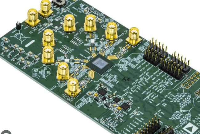
PCB layout check
1) Whether the size of the circuit board meets the processing size required by the product drawing.
2) Whether the layout of the components is balanced, neatly arranged, and well arranged.
3) Whether there are conflicts at all levels. For example, components, frames and silk screens should be reasonable.
4) Common components are easy to use. Such as switches, plug-in devices, components that must be replaced frequently, etc.
5) Whether the distance between thermal components and heating components is reasonable.
6) Whether the heat dissipation is good.
7) Whether the line interference problem needs to be considered.
PCB design, there are multiple steps you can take to minimize EMF noise/interference. The best way is to design the conductive traces in a way that minimizes EMF.
When improperly routed traces can act as antennas for EMF, to avoid EMF interfering with your traces, you can refer to the following:
1) Keep traces as short as possible;
2) Avoid creating loops with traces;
3) Avoid bends in traces at 90° angles (use 45° angles instead);
4) Separate high-speed signals from low-speed signals;
5) Keep return paths short;
6) Route differential (+/-) traces as close to each other as possible.