
PCB Solder Mask: A Comprehensive Guide to Design, Application, and Optimization
The solder mask, also known as the solder resist or solder stop mask, is a critical layer in PCB (Printed Circuit Board) manufacturing. It is a thin, protective coating applied over the copper traces to prevent oxidation, protect against environmental factors, and ensure proper soldering during assembly. The solder mask also plays a key role in defining the solderable areas of the PCB, preventing solder bridges, and improving the overall reliability of the board. This article provides a comprehensive guide to PCB solder mask design, application, and optimization, covering its purpose, types, materials, design considerations, and best practices.
1. Introduction to PCB Solder Mask
The solder mask is a polymer layer applied to the PCB surface, leaving only the exposed pads and vias for soldering. It serves several essential functions:
- Protection: Prevents oxidation and corrosion of copper traces.
- Insulation: Provides electrical insulation between adjacent traces.
- Solder Control: Defines solderable areas and prevents solder bridging.
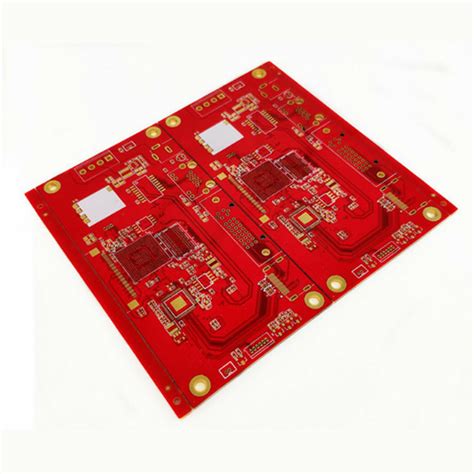
- Aesthetic Enhancement: Improves the visual appearance of the PCB with colored coatings (e.g., green, blue, red, or black).
The solder mask is applied after the copper traces are etched and before the surface finish is applied. Its design and quality directly impact the manufacturability, reliability, and performance of the PCB.

2. Types of Solder Mask
2.1 Liquid Photoimageable Solder Mask (LPSM)
LPSM is the most commonly used type of solder mask. It is applied as a liquid and then exposed to UV light through a photomask to define the solderable areas.
- Advantages: High resolution, excellent adhesion, and compatibility with fine-pitch components.
- Disadvantages: Requires precise application and curing processes.
- Applications: High-density PCBs, consumer electronics, and industrial controls.
2.2 Dry Film Solder Mask (DFSM)
DFSM is a solid film laminated onto the PCB surface and then exposed to UV light through a photomask.
- Advantages: Uniform thickness, good for high-volume production.
- Disadvantages: Limited flexibility, not suitable for complex geometries.
- Applications: High-volume, low-complexity PCBs.
2.3 Epoxy-Based Solder Mask
Epoxy-based solder masks are applied as a liquid and cured using heat or UV light. They are less common but offer excellent mechanical and chemical resistance.
- Advantages: High durability and chemical resistance.
- Disadvantages: Lower resolution compared to LPSM.
- Applications: Harsh environments, automotive, and aerospace.
3. Solder Mask Materials
The choice of solder mask material depends on the application, performance requirements, and manufacturing process. Common materials include:
3.1 Epoxy Resins
Epoxy resins are the most widely used solder mask materials due to their excellent adhesion, durability, and chemical resistance.
- Advantages: High mechanical strength, good thermal stability.
- Disadvantages: Limited flexibility, higher cost.
- Applications: General-purpose PCBs, industrial controls.
3.2 Acrylic Resins
Acrylic resins are used for their flexibility and ease of application.
- Advantages: Good flexibility, lower cost.
- Disadvantages: Lower thermal and chemical resistance.
- Applications: Flexible PCBs, consumer electronics.
3.3 Polyimide Resins
Polyimide resins are used in high-temperature and high-reliability applications.
- Advantages: Excellent thermal stability, high chemical resistance.
- Disadvantages: High cost, difficult to process.
- Applications: Aerospace, military, and high-temperature environments.
4. Design Considerations for Solder Mask
4.1 Solder Mask Clearance
Solder mask clearance refers to the gap between the solder mask and the exposed copper pads. Proper clearance is critical to ensure reliable soldering and prevent solder mask encroachment.
- Standard Clearance: Typically 0.05-0.1 mm (2-4 mils) around pads.
- Fine-Pitch Components: May require tighter clearance (e.g., 0.025 mm or 1 mil).
4.2 Solder Mask Defined (SMD) vs. Non-Solder Mask Defined (NSMD) Pads
- SMD Pads: The solder mask defines the pad size, leaving a smaller exposed copper area. This provides better mechanical strength but may reduce solderability.
- NSMD Pads: The copper defines the pad size, providing better solderability but lower mechanical strength.
4.3 Solder Mask Thickness
The thickness of the solder mask affects its protective and insulating properties.
- Standard Thickness: 0.01-0.03 mm (0.4-1.2 mils).
- High-Density PCBs: Thinner solder masks (e.g., 0.01 mm or 0.4 mils) are used to accommodate fine-pitch components.
4.4 Solder Mask Color
While green is the most common solder mask color, other colors (e.g., blue, red, black, white) are available for aesthetic or functional purposes.
- Green: Standard color, provides good contrast for inspection.
- Blue/Red/Black: Used for branding or aesthetic purposes.
- White: Used for LED PCBs to reflect light.
5. Best Practices for Solder Mask Design
5.1 Follow Manufacturer Guidelines
Always adhere to the PCB manufacturer’s design rules for solder mask clearance, thickness, and material selection.
5.2 Optimize Solder Mask Clearance
Ensure adequate clearance around pads to prevent solder mask encroachment and ensure reliable soldering.
5.3 Use SMD Pads for BGA Components
For BGA (Ball Grid Array) components, use SMD pads to improve mechanical strength and prevent solder ball detachment.
5.4 Avoid Solder Mask on Test Points
Leave test points and debug pads exposed to allow for easy probing and testing.
5.5 Consider Thermal Management
Use solder mask openings to expose thermal pads and improve heat dissipation for high-power components.
6. Common Challenges and Solutions
6.1 Solder Mask Bridging
- Challenge: Solder mask material bridges between pads, causing soldering issues.
- Solution: Increase solder mask clearance or adjust the application process.
6.2 Solder Mask Voids
- Challenge: Voids or bubbles in the solder mask layer reduce protection.
- Solution: Ensure proper surface preparation and application techniques.
6.3 Solder Mask Peeling
- Challenge: Solder mask peels off due to poor adhesion.
- Solution: Use high-quality materials and ensure proper curing.
7. Emerging Trends in Solder Mask Technology
7.1 High-Resolution Solder Masks
Advances in solder mask materials and application techniques are enabling higher resolution for fine-pitch components.
7.2 Flexible Solder Masks
Flexible solder masks are being developed for use in flexible and rigid-flex PCBs.
7.3 Environmentally Friendly Materials
New solder mask materials are being developed to meet environmental regulations, such as RoHS and REACH.
8. Conclusion
The solder mask is a critical component of PCB design and manufacturing, providing protection, insulation, and solder control. By understanding the types, materials, and design considerations associated with solder masks, engineers can optimize their PCBs for performance, reliability, and manufacturability. Emerging trends, such as high-resolution and flexible solder masks, are driving innovation in the industry, offering new possibilities for advanced PCB designs. With careful attention to detail and adherence to best practices, solder mask design can be optimized to meet the demands of modern electronics.