
USB on PCB: Design, Implementation, and Best Practices
Introduction
Universal Serial Bus (USB) has become one of the most widely used interfaces for connecting peripherals to computers and other electronic devices. Its versatility, ease of use, and high data transfer rates have made it a standard in modern electronics. When designing a printed circuit board (PCB) that incorporates USB functionality, engineers must consider various factors to ensure reliable performance, signal integrity, and compliance with USB standards. This article explores the key aspects of integrating USB on a PCB, including design considerations, implementation strategies, and best practices.
1. Overview of USB Technology
USB technology has evolved significantly since its introduction in the mid-1990s. The USB Implementers Forum (USB-IF) has released several versions of the USB standard, each offering improvements in speed, power delivery, and functionality:
- USB 1.x: Introduced in 1996, with data rates of 1.5 Mbps (Low Speed) and 12 Mbps (Full Speed).
- USB 2.0: Released in 2000, supporting data rates up to 480 Mbps (High Speed).
- USB 3.x: Introduced in 2008, with data rates up to 5 Gbps (SuperSpeed) and later 10 Gbps (SuperSpeed+).
- USB4: Released in 2019, offering data rates up to 40 Gbps and compatibility with Thunderbolt 3.
In addition to data transfer, USB also provides power delivery (up to 100W with USB Power Delivery) and supports various protocols, such as USB On-The-Go (OTG) for host-device role swapping.
2. USB Interface on PCB
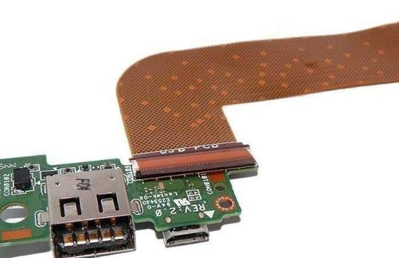
Integrating USB into a PCB involves designing the physical interface, routing the differential pairs, and ensuring proper power delivery. The USB interface typically consists of the following components:
- Connector: The physical interface that allows devices to connect to the PCB. Common types include USB Type-A, Type-B, Type-C, and micro-USB.
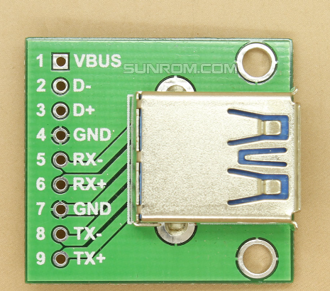
- Differential Pairs: USB data lines (D+ and D-) are transmitted as differential signals to minimize noise and improve signal integrity.
- Power Lines: VBUS (power) and GND (ground) lines provide power to connected devices.
- ESD Protection: Electrostatic discharge (ESD) protection circuits are essential to safeguard the USB interface from damage.
3. Design Considerations for USB on PCB
Designing a USB interface on a PCB requires careful attention to several factors to ensure optimal performance and compliance with USB standards.
3.1. Signal Integrity
Signal integrity is critical for USB communication, especially at higher data rates (e.g., USB 3.x and USB4). Key considerations include:
- Impedance Matching: USB differential pairs must be designed with controlled impedance (typically 90 ohms for USB 2.0 and 3.x). This requires precise trace width and spacing calculations based on the PCB stack-up.
- Trace Length Matching: The lengths of the D+ and D- traces should be matched to minimize skew and ensure proper signal timing.
- Minimizing Crosstalk: Keep USB traces away from noisy signals (e.g., clock lines) and use ground planes to reduce electromagnetic interference (EMI).
3.2. Power Delivery
USB devices often draw power from the host, so the PCB design must account for power delivery requirements:
- Voltage Drop: Ensure that the VBUS trace can handle the required current without significant voltage drop. Use wider traces or power planes if necessary.
- Decoupling Capacitors: Place decoupling capacitors near the USB connector and controller to stabilize the power supply and reduce noise.
3.3. ESD Protection
USB interfaces are exposed to external environments, making them susceptible to ESD events. Incorporate ESD protection devices (e.g., TVS diodes) near the USB connector to protect the circuitry.
3.4. EMI/EMC Compliance
USB interfaces can generate electromagnetic interference (EMI) and must comply with electromagnetic compatibility (EMC) regulations. Strategies to reduce EMI include:
- Shielding: Use shielded USB cables and connectors.
- Grounding: Ensure proper grounding of the USB connector and surrounding circuitry.
- Ferrite Beads: Add ferrite beads on power lines to suppress high-frequency noise.
4. Implementation Strategies
Implementing USB on a PCB involves selecting the right components, designing the layout, and testing the interface.
4.1. Component Selection
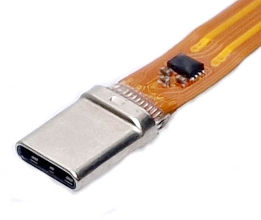
- USB Connector: Choose a connector that matches the device’s requirements (e.g., Type-C for modern devices).
- USB Controller: Select a USB controller or transceiver that supports the desired USB version and features (e.g., OTG, Power Delivery).
- Passive Components: Include resistors, capacitors, and ESD protection devices as needed.
4.2. PCB Layout
The PCB layout plays a crucial role in the performance of the USB interface:
- Differential Pair Routing: Route D+ and D- traces as closely as possible, maintaining consistent spacing and avoiding sharp bends.
- Ground Plane: Use a solid ground plane beneath the USB traces to provide a return path and reduce EMI.
- Placement: Place the USB connector and controller close to each other to minimize trace lengths and improve signal integrity.
4.3. Testing and Validation
After designing and assembling the PCB, test the USB interface to ensure it meets performance and compliance requirements:
- Signal Integrity Testing: Use tools like time-domain reflectometry (TDR) to verify impedance matching and trace integrity.
- Power Delivery Testing: Measure voltage and current levels to ensure proper power delivery.
- Compliance Testing: Perform USB-IF compliance testing to certify the design.
5. Best Practices for USB on PCB
To achieve a robust and reliable USB interface on a PCB, follow these best practices:
- Follow USB Standards: Adhere to the USB-IF specifications for your USB version.
- Use Reference Designs: Leverage reference designs and application notes from USB controller manufacturers.
- Simulate Before Fabrication: Use simulation tools to analyze signal integrity and power delivery before prototyping.
- Minimize Stubs: Avoid stubs on USB traces, as they can cause signal reflections and degrade performance.
- Test Early and Often: Conduct thorough testing at each stage of the design process to identify and address issues early.
6. Advanced Topics
For more complex designs, consider the following advanced topics:
- USB Type-C: The reversible Type-C connector supports higher power delivery, faster data rates, and alternate modes (e.g., DisplayPort, HDMI).
- USB4 and Thunderbolt: These technologies require advanced PCB materials and design techniques to support ultra-high-speed data transfer.
- USB Hubs: Designing a USB hub on a PCB involves managing multiple downstream ports and ensuring proper signal distribution.
Conclusion
Integrating USB on a PCB is a critical aspect of modern electronics design. By understanding the principles of USB technology, following design best practices, and leveraging advanced tools and techniques, engineers can create reliable and high-performance USB interfaces. Whether designing a simple USB 2.0 device or a complex USB4 system, careful attention to signal integrity, power delivery, and compliance will ensure success in today’s connected world.
This article provides a comprehensive overview of USB on PCB design, covering essential concepts, implementation strategies, and best practices. By following these guidelines, engineers can create robust and efficient USB interfaces that meet the demands of modern electronic devices.