Comprehensive Guide to PCB Flying Probe Testing
Introduction
Printed Circuit Board (PCB) manufacturing is a complex process that requires rigorous testing to ensure functionality, reliability, and performance. Among the various testing methods available, Flying Probe Testing (FPT) has emerged as a highly efficient and flexible solution for PCB validation. Unlike traditional bed-of-nails testing, flying probe testing does not require custom fixtures, making it ideal for prototyping and low-to-medium volume production.
This article explores the fundamentals of flying probe testing, its advantages, limitations, applications, and future trends in PCB manufacturing.
1. What is Flying Probe Testing?
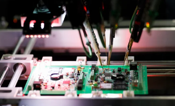
Flying Probe Testing is an automated, fixtureless testing method used to verify the electrical integrity of PCBs. Instead of using a fixed test fixture with multiple contact points (as in bed-of-nails testing), FPT employs two or more movable probes that “fly” across the board to make contact with test points.
Key Components of Flying Probe Testers
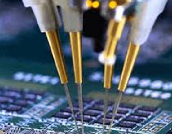
- Robotic Probes: High-precision moving probes that make electrical contact with test points.
- Software Control System: Guides the probes based on the PCB design files (Gerber, CAD, or netlist data).
- Measurement Instruments: Perform continuity, isolation, resistance, capacitance, and other electrical tests.
- Vision Systems (Optional): Some testers include cameras for alignment and component inspection.
2. How Flying Probe Testing Works
The flying probe testing process involves the following steps:
Step 1: Test Program Generation
- The PCB design files (Gerber, ODB++, or netlist) are imported into the flying probe test software.
- The software automatically generates a test program, defining probe movement paths and test sequences.
Step 2: Probe Movement & Contact
- The robotic arms position the probes onto designated test points (pads, vias, or component leads).
- The probes apply a small electrical signal to measure parameters such as:
- Continuity (ensuring connections exist where they should).
- Isolation (ensuring no unintended shorts between circuits).
- Component Values (resistance, capacitance, inductance, etc.).
Step 3: Data Analysis & Reporting
- The system compares measured values against expected thresholds.
- Defects (opens, shorts, wrong component values) are logged, and a test report is generated.
3. Advantages of Flying Probe Testing
Flying probe testing offers several benefits over traditional testing methods:
A. No Custom Fixtures Required
- Unlike bed-of-nails testing, FPT does not require expensive, custom-made test fixtures.
- This reduces setup costs and lead time, making it ideal for prototypes and small batches.
B. Flexibility & Quick Turnaround
- Test programs can be quickly modified for different PCB designs.
- Ideal for high-mix, low-volume (HMLV) production environments.
C. High Accuracy & Repeatability
- Modern flying probe testers offer micron-level positioning accuracy.
- Suitable for testing high-density PCBs with fine-pitch components.
D. Comprehensive Test Coverage
- Can test complex PCBs with BGAs, microvias, and RF circuits.
- Supports advanced measurements (impedance, high-frequency signals).
E. Cost-Effective for Low Volumes
- Eliminates fixture costs, making it economical for small production runs.
4. Limitations of Flying Probe Testing
Despite its advantages, FPT has some limitations:
A. Slower Than Fixture-Based Testing
- Since probes move sequentially, testing takes longer compared to bed-of-nails (which tests all points simultaneously).
- Not ideal for high-volume production where speed is critical.
B. Limited Power & High-Current Testing
- Flying probes are not designed for high-power or high-current testing.
- Fixture-based testers are better suited for burn-in and high-load testing.
C. Mechanical Wear & Tear
- Moving parts (probes, motors) experience mechanical wear over time, requiring maintenance.
D. Limited Analog & Functional Testing
- While FPT excels at basic electrical tests, complex functional testing may still require additional methods.
5. Applications of Flying Probe Testing
Flying probe testing is widely used in:
A. Prototype & NPI (New Product Introduction)
- Fast validation of new PCB designs without fixture delays.
B. Low-to-Medium Volume Production
- Cost-effective for small batches (e.g., aerospace, medical, automotive).
C. High-Density & Complex PCBs
- Suitable for HDI (High-Density Interconnect), flexible PCBs, and RF designs.
D. Quick Design Iterations
- Engineers can rapidly test design changes without fixture modifications.
6. Flying Probe Testing vs. Other PCB Testing Methods
| Test Method | Flying Probe Test | Bed-of-Nails Test | Automated Optical Inspection (AOI) | In-Circuit Test (ICT) |
|---|---|---|---|---|
| Fixture Required? | No | Yes | No | Yes |
| Test Speed | Slow (sequential) | Fast (parallel) | Fast (optical scan) | Fast (parallel) |
| Best For | Prototypes, low volume | High volume | Visual defects | Functional testing |
| Cost | Low (no fixture) | High (custom fixture) | Medium | High |
| Test Coverage | Electrical + some analog | Full electrical | Visual only | Full functional |
7. Future Trends in Flying Probe Testing
A. AI & Machine Learning Integration
- AI-driven defect prediction and adaptive test optimization.
B. Faster Probe Movement & Multi-Probe Systems
- Increased parallelism to reduce test time.
C. Enhanced High-Frequency Testing
- Improved RF and high-speed digital testing capabilities.
D. Integration with Industry 4.0
- Smart factory connectivity for real-time data analytics.
Conclusion
Flying Probe Testing is a versatile and cost-effective solution for PCB validation, particularly in prototyping and low-volume production. While it may not replace fixture-based testing for high-speed manufacturing, its flexibility, accuracy, and fixtureless operation make it indispensable in modern PCB manufacturing.
As technology advances, flying probe testers will continue to evolve, integrating AI, faster probing, and enhanced measurement capabilities to meet the demands of next-generation electronics.