
Key Considerations in the PCB Prototyping Process
Printed Circuit Board (PCB) prototyping is a crucial stage in electronics development, allowing engineers to test and refine designs before mass production. A well-executed PCB prototype ensures functionality, reliability, and manufacturability. However, the process involves several critical steps where mistakes can lead to costly delays or failures. This article explores the key considerations in PCB prototyping to ensure a smooth and successful outcome.
1. Design Verification Before Prototyping
Before sending a design for prototyping, thorough verification is essential to avoid errors that could render the board unusable.
a. Schematic and Layout Review
- Ensure the schematic matches the intended circuit functionality.
- Verify component footprints and pin assignments to prevent soldering issues.
- Cross-check netlists to confirm proper connections.
b. Design Rule Check (DRC)
- Run a DRC to detect spacing violations, trace width errors, and other layout issues.
- Ensure compliance with the manufacturer’s design specifications (e.g., minimum trace width, via size).
c. Signal Integrity and Power Distribution
- High-speed designs require controlled impedance traces and proper grounding.
- Use power planes and decoupling capacitors to minimize noise.
d. Thermal Management
- Ensure adequate thermal relief for high-power components.
- Avoid placing heat-sensitive parts near hot components.
2. Choosing the Right PCB Manufacturer
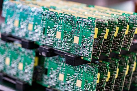
Selecting a reliable PCB fabrication partner is critical for quality prototypes.
a. Capability Assessment
- Confirm the manufacturer supports your PCB specifications (layers, materials, finishes).
- Check if they offer quick-turn prototyping for faster iterations.
b. Quality Standards
- Look for certifications like ISO 9001, UL, or IPC standards.
- Read reviews or request sample boards to assess quality.
c. Cost vs. Turnaround Time
- Balance budget constraints with required lead times.
- Some manufacturers offer discounts for small prototype batches.
3. Material Selection
The choice of PCB materials affects performance, durability, and cost.
a. Substrate Material
- FR-4: Standard for most applications, cost-effective.
- High-Frequency Materials (Rogers, PTFE): Needed for RF/microwave circuits.
- Flexible PCBs (Polyimide): Used in wearable or bendable electronics.
b. Copper Weight
- Standard PCBs use 1 oz/ft² copper; high-current designs may require 2 oz/ft² or more.
c. Surface Finish
- HASL (Hot Air Solder Leveling): Economical but not ideal for fine-pitch components.
- ENIG (Electroless Nickel Immersion Gold): Better for soldering and corrosion resistance.
- OSP (Organic Solderability Preservative): Low-cost but less durable.

4. PCB Layer Stackup Considerations
The layer stackup impacts signal integrity, EMI, and manufacturability.
a. Number of Layers
- Simple circuits: 1-2 layers.
- Complex designs: 4+ layers with dedicated power and ground planes.
b. Impedance Control
- High-speed signals require precise trace width and dielectric spacing.
- Consult the manufacturer for impedance calculations.
c. Via Types
- Through-hole vias: Standard for most PCBs.
- Blind/Buried vias: Used in HDI (High-Density Interconnect) designs.
5. Design for Manufacturability (DFM)
Optimizing the design for fabrication reduces errors and costs.
a. Minimum Trace Width and Spacing
- Follow the manufacturer’s guidelines to avoid etching issues.
b. Solder Mask and Silkscreen Clarity
- Ensure solder mask openings align with pads.
- Silkscreen should be legible and avoid component placements.
c. Panelization (for Small Boards)
- Small PCBs may be panelized for easier assembly.
- Include mouse bites or V-grooves for depanelization.
6. Testing and Validation
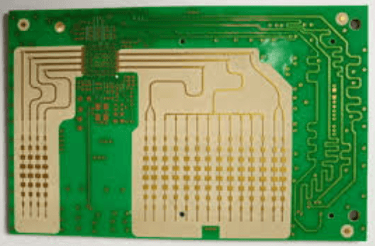
After receiving the prototype, thorough testing is necessary.
a. Visual Inspection
- Check for physical defects (scratches, misaligned drills).
- Verify solder mask and silkscreen accuracy.
b. Continuity Testing
- Use a multimeter or automated tester to confirm electrical connections.
c. Functional Testing
- Power up the board and validate performance under real conditions.
- Use oscilloscopes or logic analyzers for signal verification.
d. Environmental Stress Testing (if needed)
- Thermal cycling, vibration, or humidity tests for rugged applications.
7. Iterative Improvements
Prototyping often requires multiple iterations.
a. Documenting Issues
- Keep a log of design flaws and manufacturing feedback.
- Update schematics and layouts accordingly.
b. Cost Optimization
- Eliminate unnecessary layers or features in later revisions.
- Consider alternative components if availability is an issue.
Conclusion
PCB prototyping is a meticulous process that demands attention to design, material selection, manufacturing quality, and testing. By following these best practices, engineers can minimize errors, reduce costs, and accelerate product development. Whether for a simple hobby project or a complex industrial application, a well-planned PCB prototype ensures a smoother transition to full-scale production.
By adhering to these guidelines, designers can enhance reliability, performance, and efficiency in their PCB development cycle.