
Microwave Circuits and PCB Design: Principles and Practices
Abstract
Microwave circuits are essential components in modern communication systems, radar, satellite technology, and wireless networks. The design of microwave printed circuit boards (PCBs) requires specialized knowledge of high-frequency signal propagation, material selection, and layout techniques. This paper explores the fundamental principles of microwave circuit design, key considerations for PCB layout, and advanced techniques to minimize signal loss and electromagnetic interference (EMI). The discussion includes substrate selection, transmission line design, impedance matching, and simulation tools for optimizing microwave PCB performance.
1. Introduction
Microwave circuits operate at frequencies ranging from 1 GHz to over 100 GHz, where traditional low-frequency PCB design rules no longer apply. At these frequencies, signal integrity, parasitic effects, and electromagnetic interactions become critical challenges. Proper PCB design ensures minimal insertion loss, controlled impedance, and reduced crosstalk, which are vital for high-performance microwave applications.
This paper covers:
- Microwave PCB materials and substrates
- Transmission line structures (microstrip, stripline, coplanar waveguide)
- Impedance matching techniques
- Parasitic effects and mitigation strategies
- Simulation and testing methodologies
2. Microwave PCB Materials and Substrates
The choice of substrate material significantly impacts the performance of microwave circuits. Key parameters include:
2.1 Dielectric Constant (εᵣ)
The dielectric constant affects signal propagation speed and impedance. Common materials:
- FR-4 (εᵣ ≈ 4.3) – Low-cost but high loss at microwave frequencies.
- Rogers RO4000 series (εᵣ ≈ 3.3–6.15) – Low-loss, high-frequency laminates.
- PTFE (Teflon, εᵣ ≈ 2.1) – Excellent high-frequency performance but expensive.
2.2 Loss Tangent (tan δ)
A measure of dielectric loss. Lower values (e.g., < 0.002) are preferred for minimal signal attenuation.
2.3 Thermal Stability
Microwave PCBs must withstand thermal variations without warping or delamination.
3. Transmission Line Structures
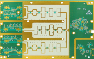
Microwave signals require controlled-impedance transmission lines to minimize reflections. Common types:
3.1 Microstrip Line
- A conductor on top of a dielectric layer with a ground plane beneath.
- Easy to fabricate but susceptible to radiation loss at high frequencies.
- Impedance depends on trace width (W), substrate height (h), and εᵣ.
3.2 Stripline
- A conductor sandwiched between two ground planes.
- Lower radiation loss but harder to fabricate.
- Used in multilayer PCBs for better EMI shielding.
3.3 Coplanar Waveguide (CPW)
- Signal trace with ground planes on the same layer.
- Lower dispersion and easier integration with surface-mount components.
4. Impedance Matching and Signal Integrity
Impedance mismatches cause signal reflections, leading to power loss and distortion.
4.1 Quarter-Wave Transformer
A λ/4 transmission line section transforms impedance to match source and load.
4.2 Stub Matching
Open or shorted stubs adjust impedance by introducing reactive components.
4.3 Tapered Lines
Gradual width transitions minimize reflections in broadband applications.
5. Parasitic Effects and Mitigation
At microwave frequencies, parasitic capacitance and inductance degrade performance.
5.1 Skin Effect
High-frequency currents flow near the conductor surface, increasing resistance.
- Solution: Use wider traces or surface plating (e.g., gold) to reduce loss.
5.2 Crosstalk
Unwanted coupling between adjacent traces.
- Solution: Increase spacing, use guard traces, or employ differential signaling.
5.3 Via Effects
Vias introduce inductance and discontinuities.
- Solution: Use multiple vias in parallel or back-drilled vias for RF grounding.
6. Simulation and Optimization Tools
Modern microwave PCB design relies on electromagnetic (EM) simulation software:
- ANSYS HFSS – 3D full-wave EM simulation.
- Keysight ADS – Circuit and EM co-simulation.
- CST Microwave Studio – Time-domain EM analysis.
Simulation helps optimize:
- S-parameters (insertion loss, return loss).
- Radiation patterns (for antenna-integrated PCBs).
- Thermal performance (power dissipation analysis).
7. Fabrication and Testing Considerations
7.1 Manufacturing Tolerances
- Tight control over trace width and dielectric thickness is critical.
- Laser drilling ensures precise via formation.
7.2 Testing Methods
- Vector Network Analyzer (VNA) measures S-parameters.
- Time-Domain Reflectometry (TDR) detects impedance discontinuities.
8. Conclusion
Designing microwave PCBs requires careful consideration of materials, transmission line structures, impedance matching, and parasitic effects. Advanced simulation tools and precise fabrication techniques are essential for achieving optimal performance. As wireless technology advances toward 5G/6G and millimeter-wave applications, microwave PCB design will continue to evolve, demanding even greater precision and innovation.