Design of Mixed-Signal PCBs: Challenges and Best Practices
Abstract
Mixed-signal printed circuit board (PCB) design integrates both analog and digital circuits on a single board, presenting unique challenges in signal integrity, power distribution, and electromagnetic compatibility (EMC). This paper explores key considerations in mixed-signal PCB design, including partitioning, grounding strategies, noise reduction techniques, and layout optimization. By following best practices, designers can mitigate interference, enhance performance, and ensure reliable operation in complex mixed-signal systems.
1. Introduction
Mixed-signal PCBs are widely used in applications such as data acquisition systems, wireless communication devices, and embedded control systems. These designs combine sensitive analog components (e.g., sensors, amplifiers, ADCs/DACs) with high-speed digital circuits (e.g., microcontrollers, FPGAs). However, the coexistence of analog and digital signals introduces challenges like crosstalk, ground bounce, and electromagnetic interference (EMI). Effective PCB design techniques are essential to maintain signal fidelity and system stability.
2. Key Challenges in Mixed-Signal PCB Design
2.1 Signal Integrity Issues
- Crosstalk: High-speed digital signals can induce noise in adjacent analog traces.
- Impedance Mismatch: Poorly controlled trace impedance leads to reflections and signal distortion.
- Return Path Discontinuities: Inadequate ground paths increase loop inductance, degrading signal quality.
2.2 Power Integrity and Noise
- Switching Noise: Digital circuits generate high-frequency noise that can couple into analog power supplies.
- Ground Loops: Improper grounding creates voltage differences, introducing noise in analog circuits.
2.3 Electromagnetic Interference (EMI)
- Radiated emissions from high-speed digital signals can interfere with analog components.
- Poor shielding and layout increase susceptibility to external noise.
3. Best Practices for Mixed-Signal PCB Design
3.1 Partitioning and Layout Strategies
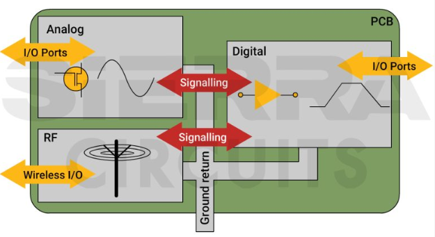
- Physical Separation: Divide the PCB into distinct analog and digital sections to minimize interference.
- Signal Routing: Route analog and digital traces perpendicularly to reduce crosstalk.
- Component Placement: Position analog components (e.g., ADCs, amplifiers) away from high-speed digital ICs.
3.2 Grounding Techniques
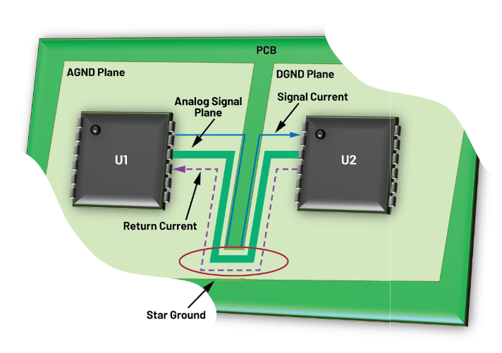
- Star Grounding: Connect all ground returns to a single point to avoid ground loops.
- Split Ground Planes: Use separate ground planes for analog and digital sections but connect them at a single point near the power supply.
- Ground Pours: Fill unused board areas with ground copper to reduce EMI.
3.3 Power Distribution and Decoupling
- Separate Power Rails: Use independent regulators for analog and digital supplies.
- Decoupling Capacitors: Place bypass capacitors close to IC power pins to filter high-frequency noise.
- Ferrite Beads: Use ferrite beads on power lines to suppress high-frequency interference.
3.4 Signal Routing and Shielding
- Differential Pair Routing: For high-speed signals, use differential pairs to reduce EMI.
- Guard Traces: Place grounded guard traces around sensitive analog signals to block noise.
- Shielding: Use metal shields or grounded copper layers to isolate critical analog sections.
3.5 PCB Stackup Considerations
- Multi-Layer Boards: Use at least four layers (signal, ground, power, signal) to improve noise immunity.
- Dedicated Ground Plane: Ensure a low-impedance return path for high-frequency signals.
- Controlled Impedance Traces: Match trace impedance to prevent signal reflections.
4. Simulation and Verification
Before fabrication, mixed-signal PCB designs should undergo:
- SPICE Simulations: Analyze analog circuit behavior under different conditions.
- Signal Integrity (SI) Analysis: Check for reflections, crosstalk, and timing issues.
- EMI/EMC Testing: Verify compliance with electromagnetic compatibility standards.
5. Case Study: Mixed-Signal Data Acquisition System
A 16-bit ADC interfacing with a microcontroller was designed using:
- Partitioning: Analog front-end placed on one side, digital processing on the other.
- Grounding: Single-point connection between analog and digital grounds.
- Decoupling: Multiple 0.1µF and 10µF capacitors near ADC and MCU.
- Results: Achieved SNR > 90dB with minimal digital noise coupling.
6. Conclusion
Designing mixed-signal PCBs requires careful consideration of layout, grounding, power distribution, and noise reduction. By implementing proper partitioning, shielding, and simulation techniques, engineers can optimize performance and reliability in mixed-signal applications. Future advancements in high-speed ADCs, low-noise amplifiers, and advanced PCB materials will further enhance mixed-signal design capabilities.