Machine Vision in Comprehensive Inspection of PCB Circuit Boards
Abstract
Machine vision technology has become an indispensable tool in the manufacturing and quality control of printed circuit boards (PCBs). With the increasing complexity and miniaturization of electronic components, traditional manual inspection methods are no longer sufficient to ensure high precision and efficiency. This paper explores the applications of machine vision in PCB inspection, including defect detection, component placement verification, solder joint inspection, and dimensional measurement. The advantages of machine vision, such as high speed, accuracy, and repeatability, make it a critical technology in modern PCB manufacturing. Additionally, challenges and future trends in machine vision-based PCB inspection are discussed.
1. Introduction
Printed circuit boards (PCBs) are the backbone of modern electronic devices, serving as the platform for interconnecting various electronic components. The quality and reliability of PCBs directly impact the performance of electronic products. As PCBs become more complex with higher component density and finer traces, traditional inspection methods, such as manual visual checks, are prone to human error and inefficiency.
Machine vision, a technology that uses cameras, image processing algorithms, and artificial intelligence (AI), has emerged as a powerful solution for automated PCB inspection. It enables high-speed, non-contact, and highly accurate defect detection, ensuring consistent quality in mass production. This paper examines the key applications of machine vision in PCB inspection, its benefits, and future advancements.
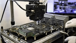
2. Key Applications of Machine Vision in PCB Inspection
2.1 Defect Detection
One of the primary applications of machine vision in PCB manufacturing is defect detection. Common PCB defects include:
- Short circuits and open circuits – Machine vision systems can detect unintended connections (shorts) or broken traces (opens) by analyzing high-resolution images of the PCB.
- Solder bridging – Excessive solder between adjacent pins can cause electrical shorts, which machine vision can identify through precise image analysis.
- Missing or misaligned components – Automated optical inspection (AOI) systems verify the presence and correct placement of components by comparing captured images with reference designs.
- Contamination and scratches – Foreign particles or physical damage on the PCB surface can be detected using specialized lighting and image processing techniques.
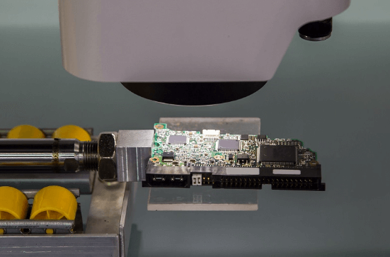
2.2 Component Placement Verification
Surface-mount technology (SMT) has led to the miniaturization of electronic components, making manual inspection impractical. Machine vision systems ensure that components are correctly placed and aligned before soldering. Key inspection points include:
- Component presence/absence – Confirming that all required components are mounted.
- Polarity and orientation – Ensuring diodes, capacitors, and ICs are correctly oriented.
- Alignment accuracy – Verifying that components are placed within acceptable tolerances.
2.3 Solder Joint Inspection
Solder joint quality is critical for electrical connectivity and mechanical stability. Machine vision systems inspect solder joints for defects such as:
- Insufficient or excessive solder – Automated systems measure solder volume to ensure proper connections.
- Voids and cracks – X-ray machine vision can detect internal defects in solder joints.
- Cold solder joints – Poor wetting or incomplete melting can be identified through thermal imaging or high-resolution cameras.
2.4 Dimensional and Metrology Measurements
PCBs must adhere to strict dimensional tolerances to ensure proper fit and function in electronic assemblies. Machine vision systems perform precise measurements of:
- Trace width and spacing – Ensuring compliance with design specifications.
- Hole diameter and position – Verifying drill accuracy for through-hole components.
- Board warpage and flatness – Detecting deformations that could affect assembly.
3. Advantages of Machine Vision in PCB Inspection
The adoption of machine vision in PCB inspection offers several benefits:
- High Speed and Efficiency – Machine vision systems can inspect hundreds of PCBs per minute, far exceeding manual inspection capabilities.
- Improved Accuracy – AI-powered algorithms detect micron-level defects that human inspectors might miss.
- Consistency and Repeatability – Unlike human inspectors, machine vision does not suffer from fatigue or subjective judgment.
- Cost Reduction – Automated inspection reduces labor costs and minimizes scrap by catching defects early.
- Data Logging and Traceability – Inspection results can be stored for quality control and process optimization.
4. Challenges and Future Trends
Despite its advantages, machine vision in PCB inspection faces challenges:
- Complexity in High-Density PCBs – As components shrink, higher-resolution cameras and more advanced algorithms are needed.
- Reflective and Low-Contrast Surfaces – Special lighting techniques (e.g., coaxial or polarized lighting) are required to enhance image clarity.
- Integration with Industry 4.0 – Future systems will leverage IoT and AI for real-time defect classification and predictive maintenance.
Emerging trends include:
- Deep Learning for Defect Classification – Convolutional neural networks (CNNs) improve defect recognition accuracy.
- 3D Machine Vision – Enables better inspection of solder joints and warpage.
- In-Line Automated Inspection – Combining AOI with robotic systems for real-time corrections.
5. Conclusion
Machine vision has revolutionized PCB inspection by enabling fast, accurate, and automated quality control. Its applications in defect detection, component verification, solder joint inspection, and metrology ensure high manufacturing standards. As PCB technology advances, machine vision systems will continue to evolve with AI, 3D imaging, and smart factory integration, further enhancing production efficiency and reliability.