
How Are PCB Boards Made? A Comprehensive Guide to the PCB Manufacturing Process
Printed Circuit Boards (PCBs) are the backbone of modern electronics, found in everything from smartphones and laptops to medical devices and aerospace systems. But how exactly are these intricate boards manufactured? This article explores the step-by-step process of PCB fabrication, covering design, material selection, etching, drilling, plating, and final assembly.
1. Introduction to PCB Manufacturing
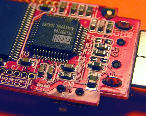
A PCB is a layered structure made of insulating materials (substrates) and conductive copper traces that connect electronic components. The manufacturing process involves multiple stages, each requiring precision and quality control to ensure reliability.
2. PCB Design and File Preparation
Before production begins, engineers design the PCB using specialized software like:
- Altium Designer
- KiCad
- Eagle
- OrCAD
The design includes:
- Schematic Capture – Defining electrical connections.
- PCB Layout – Arranging components and routing traces.
- Gerber Files – Standard manufacturing files sent to PCB fabricators.
Once the design is finalized, manufacturers perform a Design for Manufacturability (DFM) check to ensure feasibility.
3. Material Selection
PCBs are made from several key materials:
- Substrate (Base Material): Typically FR-4 (fiberglass-reinforced epoxy laminate).
- Copper Foil: Used for conductive traces (usually 1 oz/ft² to 2 oz/ft²).
- Solder Mask: A protective layer (usually green, but other colors are available).
- Silkscreen: Text and symbols printed on the board for component placement.
4. PCB Fabrication Process Step-by-Step
Step 1: Printing the PCB Design
The Gerber files are used to print the circuit pattern onto a photoresist film or directly onto the copper-clad laminate using a laser plotter.
Step 2: Copper Etching
The unwanted copper is removed using a chemical etching process:
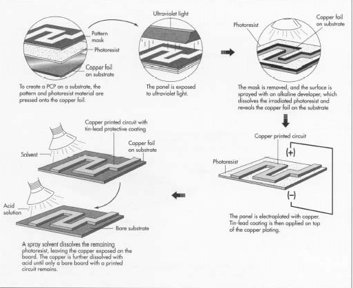
- Lamination: A photosensitive dry film is applied to the copper layer.
- Exposure to UV Light: The PCB is exposed to UV light through the photomask, hardening the desired traces.
- Developing: The unexposed photoresist is washed away.
- Etching: A chemical solution (ferric chloride or ammonium persulfate) dissolves the unprotected copper, leaving only the desired traces.
Step 3: Drilling Holes
Precision CNC drilling machines create holes for:
- Through-Hole Components (leads passing through the board).
- Vias (conductive pathways between layers).
Step 4: Plating and Copper Deposition
To ensure conductivity in drilled holes:
- Electroless Copper Deposition: A thin copper layer is chemically deposited inside the holes.
- Electroplating: Additional copper is electroplated to strengthen the connections.
Step 5: Applying the Solder Mask
A solder mask (usually green) is applied to:
- Protect copper traces from oxidation.
- Prevent solder bridges during assembly.
- Provide insulation.
The process involves:
- Coating with Liquid Photo-Imageable Solder Mask (LPI).
- Exposing to UV Light (using a solder mask stencil).
- Developing to remove unexposed areas.
Step 6: Silkscreen Printing
A silkscreen layer is added for:
- Component labels.
- Reference designators.
- Company logos.
This is typically done using inkjet printing or screen printing.
Step 7: Surface Finish Application
To protect exposed copper and improve solderability, a surface finish is applied:
- HASL (Hot Air Solder Leveling) – Traditional lead-based or lead-free solder coating.
- ENIG (Electroless Nickel Immersion Gold) – Gold plating for high reliability.
- OSP (Organic Solderability Preservative) – A thin organic coating.
Step 8: Electrical Testing and Quality Control
Before shipment, PCBs undergo:
- Automated Optical Inspection (AOI) – Checks for defects.
- Flying Probe Testing – Verifies electrical connectivity.
- Impedance Testing (for high-speed designs).
5. PCB Assembly (PCBA)
After fabrication, components are mounted via:
- Surface Mount Technology (SMT) – Automated pick-and-place machines attach components.
- Through-Hole Technology (THT) – Manual or wave soldering for larger components.
6. Final Inspection and Packaging
The assembled PCB undergoes:
- Functional Testing – Ensures the board operates correctly.
- Burn-In Testing – Stress testing under high temperatures.
- Packaging – Anti-static bags or vacuum sealing for shipping.
7. Conclusion
PCB manufacturing is a complex, multi-stage process requiring precision engineering and strict quality control. From design and material selection to etching, drilling, and final assembly, each step ensures the board meets industry standards. As technology advances, PCB fabrication continues to evolve, enabling smaller, faster, and more reliable electronic devices.
Would you like additional details on any specific step in the PCB manufacturing process?