
Optimal RF Layout Strategies for Mobile Phone PCB Design
Introduction
In the rapidly evolving world of mobile communication technology, the design of printed circuit boards (PCBs) for smartphones presents unique challenges, particularly when it comes to radio frequency (RF) circuitry. With consumers demanding ever-faster data rates, lower latency, and more reliable connections in increasingly compact form factors, RF PCB layout has become one of the most critical aspects of modern smartphone design. This 2000-word article explores best practices for RF layout in mobile phone PCB design, covering fundamental principles, component placement strategies, routing techniques, grounding methods, and advanced considerations for multi-radio systems.
Fundamental RF Layout Principles for Mobile Phones
Understanding RF Signal Characteristics
RF signals in mobile phones operate at frequencies ranging from several hundred MHz for sub-1GHz bands up to several GHz for 5G mmWave applications. These high-frequency signals exhibit behaviors significantly different from digital or low-frequency analog signals:
- Transmission Line Effects: At RF frequencies, PCB traces act as transmission lines rather than simple conductors, requiring careful impedance control.
- Skin Effect: Current tends to flow near the surface of conductors at high frequencies, increasing effective resistance.
- Parasitic Effects: Even small capacitances and inductances in the layout can significantly impact circuit performance.
Key Performance Metrics
Mobile phone RF layouts must optimize several critical parameters:
- Insertion Loss: Minimizing signal attenuation through the RF path
- Return Loss: Ensuring proper impedance matching to prevent reflections
- Noise Figure: Maintaining signal-to-noise ratio in receive chains
- Isolation: Preventing unwanted coupling between different RF sections
- Radiation Efficiency: Maximizing antenna performance while minimizing board effects
Strategic Component Placement for RF Circuits
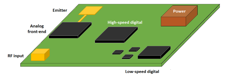
Partitioning the PCB
Effective RF layout begins with intelligent partitioning of the mobile phone PCB:
- RF Section Isolation: Dedicate a specific area of the board exclusively for RF components, physically separated from digital and power supply sections.
- Front-End Module Placement: Position RF front-end modules (FEMs) near the antenna interface to minimize transmission line losses.
- Transceiver Location: Place the RF transceiver IC centrally to balance the lengths of transmit and receive paths.
- Antenna Feed Point: Carefully consider the antenna connection point, typically at a board edge or corner for optimal radiation.
Critical Component Placement Guidelines
- Power Amplifiers (PAs): Locate PAs close to antenna switches with minimal intervening trace length
- Low-Noise Amplifiers (LNAs): Position LNAs near the antenna switch in receive paths
- Filters: Place filters immediately after PAs in transmit chains and before LNAs in receive chains
- Matching Networks: Implement matching components as close as possible to the devices they serve
- Decoupling Capacitors: Mount bypass capacitors adjacent to IC power pins with minimal lead length
RF Routing Techniques for Mobile PCBs
Transmission Line Design
Proper transmission line implementation is essential for RF signal integrity:
- Controlled Impedance Routing:
- Use microstrip or stripline configurations with calculated widths for target impedance (typically 50Ω)
- Account for dielectric constant and thickness of PCB materials
- Maintain consistent impedance throughout the RF path
- Corner Handling:
- Use curved traces or 45° miters for right-angle bends
- Avoid sharp 90° turns which cause impedance discontinuities
- Layer Stackup Considerations:
- Route critical RF signals on top layers when possible to minimize via effects
- Use adjacent ground planes for microstrip configurations
- For stripline, ensure symmetrical placement between ground planes
Crosstalk Mitigation
- Adequate Spacing: Maintain at least 3x trace width between parallel RF lines
- Orthogonal Routing: Route crossing traces on different layers at right angles
- Guard Traces: Implement grounded copper between sensitive RF lines when space permits
- Shielding: Use grounded metal shields or “copper fences” around critical RF sections
Via Management
Vias introduce discontinuities that can degrade RF performance:
- Minimize Via Count: Use the fewest vias possible in RF paths
- Via Size: Use smaller diameter vias for less inductance
- Return Path Vias: Place ground vias adjacent to signal vias for proper return current
- Antenna Vias: For internal antennas, optimize via placement for radiation efficiency

Grounding Strategies for RF Circuits
RF Ground Plane Implementation
- Dedicated Ground Layer: Use a continuous, unbroken ground plane beneath RF components
- Multi-layer Considerations: In complex boards, ensure low-impedance ground connections between layers
- Ground Isolation: Separate RF ground from digital ground, connecting at a single point when necessary
Component Grounding
- Direct Ground Connections: Provide shortest possible paths for component ground pins
- Thermal Relief Avoidance: Do not use thermal relief patterns on RF ground connections
- Ground Via Placement: Use multiple vias for low-inductance grounding of components and shields
Power Distribution for RF Circuits
Decoupling Network Design
- Multi-stage Decoupling: Implement parallel capacitors of different values (e.g., 100pF, 1nF, 10nF)
- Proximity: Place decoupling capacitors as close as possible to power pins
- High-Frequency Capacitors: Use capacitors with low equivalent series inductance (ESL)
Power Plane Considerations
- Localized Power Islands: Create small power planes for RF sections when possible
- Filtering: Implement π-filters or T-filters for clean RF power supplies
- Separation: Keep RF power traces away from digital power distribution
Advanced Considerations for Modern Smartphones
Multi-Radio Coexistence
5G mmWave Design Challenges
- Antenna Array Placement: Optimize placement of phased array antennas for beamforming
- Extreme Frequency Considerations: Account for transmission losses at 24GHz and above
- Material Selection: Use low-loss PCB materials for mmWave circuits
EMI/EMC Considerations
- Shielding Effectiveness: Design shields with proper grounding and seam placement
- Board Edge Effects: Manage fringing fields at PCB edges
- Clock Harmonic Management: Filter or shield clocks that might interfere with RF bands
Simulation and Verification
Pre-Layout Simulation
- Schematic-Level Analysis: Verify basic performance before layout
- Component Model Accuracy: Use manufacturer-provided models for critical components
- Initial Impedance Calculations: Determine target trace geometries
Post-Layout Analysis
- EM Simulation: Perform full-wave electromagnetic simulation of critical RF paths
- Signal Integrity Verification: Analyze insertion loss, return loss, and isolation
- Thermal Analysis: Evaluate power dissipation in RF components
Prototype Testing
- Network Analyzer Measurements: Verify S-parameters of RF paths
- Spectrum Analysis: Check for spurious emissions and noise
- Real-World Performance Testing: Evaluate call quality, data throughput, and battery life
Conclusion
Effective RF layout in mobile phone PCB design requires careful attention to transmission line theory, component placement, routing techniques, and grounding strategies. As smartphones continue to incorporate more radios and higher frequency bands, the challenges of RF design grow increasingly complex. By following the fundamental principles outlined in this article—proper partitioning, controlled impedance routing, meticulous grounding, and thorough verification—designers can create mobile PCBs that deliver optimal RF performance while meeting the stringent size and power constraints of modern smartphones. The key to success lies in treating the RF layout not as an afterthought, but as a central consideration from the earliest stages of the design process. With 5G and future wireless technologies pushing the boundaries of mobile communication, mastery of RF PCB layout techniques will remain an essential skill for mobile device engineers.