
PCB Design Essentials: How to Minimize Ground Noise
Introduction
Printed Circuit Board (PCB) design plays a critical role in ensuring the performance, reliability, and signal integrity of electronic devices. One of the most common challenges PCB designers face is ground noise, which can lead to signal degradation, electromagnetic interference (EMI), and even system failures.
Ground noise occurs when unwanted voltage fluctuations or currents flow through the ground plane, creating interference with sensitive circuits. To mitigate this issue, PCB designers must follow best practices in layout, grounding strategies, and component placement.
In this article, we will explore the key considerations for reducing ground noise in PCB design, including:
- Understanding Ground Noise and Its Causes
- Proper Grounding Techniques
- PCB Layout Best Practices
- Decoupling and Filtering Strategies
- Advanced Techniques for Noise Reduction
1. Understanding Ground Noise and Its Causes
Ground noise, also known as ground bounce or ground loop interference, arises due to several factors:
Common Causes of Ground Noise
- Impedance in Ground Paths: High resistance or inductance in ground traces can cause voltage drops, leading to noise.
- Return Current Path Disruptions: Poorly designed return paths force currents to take unintended routes, inducing noise.
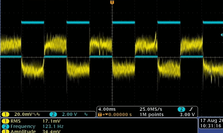
- Switching Noise (ΔI Noise): High-speed digital circuits generate rapid current changes, creating transient voltage spikes in the ground plane.
- Mixed-Signal Interference: Analog and digital circuits sharing the same ground can introduce noise through coupling.
- EMI from External Sources: Radiated or conducted interference from other components or external devices can corrupt ground integrity.
Understanding these sources helps designers implement effective countermeasures.
2. Proper Grounding Techniques
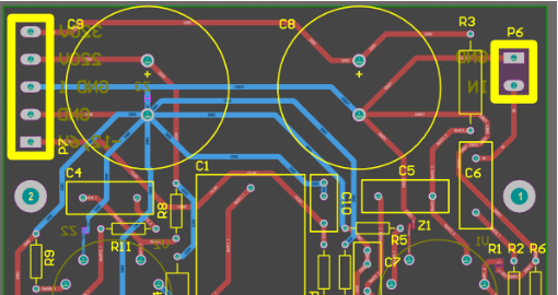
A well-designed grounding system is essential for minimizing noise. Key grounding strategies include:
a) Star Grounding
- Concept: All ground connections meet at a single point (like a star) to prevent ground loops.
- Best for: Low-frequency analog circuits where ground loops are a major concern.
b) Ground Plane Design
- Use a Solid Ground Plane: A continuous copper plane provides a low-impedance return path for currents.
- Avoid Splits in Critical Areas: Splits can force return currents to take long detours, increasing inductance and noise.
c) Separate Analog and Digital Grounds
- Problem: Digital circuits generate high-frequency noise that can couple into analog signals.
- Solution: Use separate ground planes for analog and digital sections, connecting them at a single point near the power supply.
d) Multi-Layer PCB Grounding
- Dedicated Ground Layers: In multi-layer PCBs, a full ground plane minimizes loop inductance.
- Adjacent Signal and Ground Layers: Place signal layers next to ground planes to reduce crosstalk and EMI.
3. PCB Layout Best Practices
The PCB layout significantly impacts ground noise. Follow these guidelines:
a) Minimize Ground Loop Areas
- Keep Return Paths Short: Ensure high-speed signals have a direct return path beneath them on the ground plane.
- Avoid Daisy-Chaining Grounds: This increases loop inductance and noise coupling.
b) Component Placement
- Group Components by Function: Place analog, digital, and power sections separately to reduce interference.
- Keep High-Speed Traces Away from Sensitive Signals: Route clock and data lines carefully to prevent coupling.
c) Trace Routing Considerations
- Use Short and Wide Traces for High Current Paths: Reduces inductance and resistance.
- Avoid 90° Angles in Traces: Use 45° angles or curves to minimize reflections and EMI.
d) Via Placement for Ground Connections
- Use Multiple Vias for Ground Connections: Reduces impedance and improves heat dissipation.
- Avoid Stubs in High-Speed Signals: Stub vias can cause signal reflections.
4. Decoupling and Filtering Strategies
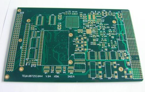
Proper decoupling and filtering are crucial for suppressing noise.
a) Decoupling Capacitors
- Place Capacitors Close to IC Power Pins: Reduces high-frequency noise by providing a local charge reservoir.
- Use Multiple Capacitor Values: Combine bulk (10μF), mid-range (0.1μF), and high-frequency (1nF) capacitors for wideband filtering.
b) Ferrite Beads and Inductors
- Use for Power Line Filtering: Blocks high-frequency noise while allowing DC to pass.
- Place Near Noise Sources: Effective for switching regulators and clock circuits.
c) RC Filters for Sensitive Signals
- Low-Pass Filters: Reduce high-frequency noise in analog signals.
- Place Near ADC/DAC Inputs: Improves signal integrity in mixed-signal designs.
5. Advanced Techniques for Noise Reduction
For high-performance or high-frequency designs, consider these advanced methods:
a) Guard Traces and Shielding
- Guard Rings for Analog Signals: A grounded trace surrounding sensitive signals prevents noise coupling.
- Shielded Enclosures: Metal shields block external EMI.
b) Differential Signaling
- Use Differential Pairs (e.g., USB, LVDS): Rejects common-mode noise.
- Ensure Tight Coupling Between Pairs: Minimizes EMI susceptibility.
c) Power Integrity Analysis
- Simulate Power Delivery Networks (PDN): Tools like HyperLynx or SIwave help identify ground noise issues.
- Check Impedance of Ground Planes: Ensures low impedance across all frequencies.
d) EMI/EMC Compliance Testing
- Pre-Compliance Testing: Identify noise issues early using spectrum analyzers and near-field probes.
- Follow EMC Design Guidelines: Ensures the PCB meets regulatory standards.
Conclusion
Reducing ground noise in PCB design requires a combination of proper grounding techniques, strategic layout practices, and effective filtering. By understanding the sources of noise and implementing best practices—such as using ground planes, separating analog and digital grounds, optimizing decoupling, and employing advanced shielding—PCB designers can significantly improve signal integrity and system reliability.
As electronic devices continue to operate at higher speeds and with greater complexity, mastering these techniques becomes even more critical. By following these guidelines, designers can minimize ground noise and ensure robust, high-performance PCB designs.