Skip to content
Andwin Circuits
  • Home
  • ProductsExpand
    • HDI multilayer PCB
    • Rigid Flex PCB
    • Flex pcb
    • Special PCBExpand
      • High Frequency PCBExpand
        • Rogers RO4350B PCB
        • Rogers RO4003 pcb
        • Rogers RO3003 PCB
        • Rogers 5880 PCB
        • DICLAD 527 PCB
        • Taconic TLX series
        • Taconic TLX-8 RF PCB
        • Taconic TLX-9 RF PCB
      • High speed pcbExpand
        • Megtron 6 High Speed PCB
        • TU-872 SLK Sp High Speed
      • High TG PCBExpand
        • SHENGYI SH260 PCB
        • ISOLA 370HR PCB
        • ISOLA IS410 PCB
        • ISOLA IS420 PCB
      • Heavy copper PCB
      • Copper coin pcb
      • Copper inlay PCB
    • Metal Core PCBExpand
      • Copper core pcb
      • Aluminum PCB
      • 2 Layers Aluminum PCB
      • Direct thermal MCPCB
      • 2 Layers Direct Thermal
    • Ceramic PCBExpand
      • DPC ceramic PCB
      • DBC ceramic PCB
      • Thick film Ceramic PCB
      • Al2O3 Alumina PCB
      • AIN ALN ceramic PCB
      • IGBT Ceramic PCB
  • ServiceExpand
    • PCB Assembly
    • Quick turn PCB assembly
    • PCBA conformal coating
  • IndustryExpand
    • Telecommunication
    • IoT and Wireless
    • Industrial Control
    • Thermal management
    • Power and Energy
    • IC test board
    • Automative
    • Medical
  • CapabilityExpand
    • Rigid PCB
    • Rigid flex PCB
    • Metal core PCB
    • PCB Assembly
  • TechnologyExpand
    • Blogs
    • Via in pad
    • PCB E-test
    • PCB stack up
    • MCPCB panelization
    • Controlled impedance PCB
  • AboutExpand
    • About us
    • Certification
    • Factory Tour
  • Contact
Andwin Circuits
Home / How to design PCB for electromagnetic interference

How to design PCB for electromagnetic interference

ByGrace July 2, 2025July 7, 2025

The frequency of electronic signals and processors of electronic equipment is constantly increasing, and the electronic system has become a complex device containing multiple components and many subsystems. High density and high speed will increase the radiation of the system, while low voltage and high sensitivity will reduce the anti-interference of the system. Therefore, electromagnetic interference (EMI) is a real threat to the safety, reliability and stability of electronic equipment. When we design electronic products, the design of PCB boards is crucial to solving EMI problems. This article mainly explains the points to pay attention to when designing PCBs, so as to reduce the electromagnetic interference problems in PCB boards.

Definition of electromagnetic interference (EMI)

Electromagnetic interference (EMI, Electro Magnetic Interference) can be divided into radiation and conduction interference. Radiated interference is the interference source using space as a medium to interfere with its signal to another electrical network. And conducted interference is the interference of the signal on one electrical network to another electrical network using a conductive medium as a medium. In high-speed system design, integrated circuit pins, high-frequency signal lines and various plugs are common radiation interference sources in PCB board design. The electromagnetic waves they emit are electromagnetic interference (EMI), which will affect the normal operation of themselves and other systems.

Contact us for PCB quote now |

PCB design tips for electromagnetic interference (EMI)

There are many solutions to EMI problems in PCB design tips today, such as EMI suppression coatings, suitable EMI suppression parts and EMI simulation design. The above video introduces methods to reduce EMI. Now let’s briefly explain these tips.

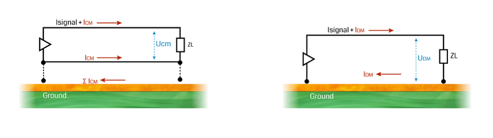
Tip 1: Common-mode EMI interference source (such as the voltage drop formed by the transient voltage formed on the power bus at both ends of the inductor of the decoupling path)

  • Use low-value inductors on the power layer, and the transient signals synthesized by the inductors will be reduced, thereby reducing common-mode EMI.
  • Reduce the length of the connection from the power layer to the IC power pin.
  • Use 3-6 mil PCB layer spacing and FR4 dielectric material.
Contact us for PCB quote now |

Tip 2: Electromagnetic shielding

  • Try to put the signal traces on the same PCB layer, and close to the power layer or ground layer.
  • The power layer should be as close to the ground layer as possible

Skill 3: Layout of parts (different layouts will affect the interference and anti-interference ability of the circuit)

  • Block processing according to different functions in the circuit (such as demodulation circuit, high-frequency amplification circuit and mixing circuit, etc.), in this process, separate strong and weak electrical signals, and separate digital and analog signal circuits
  • The filter network of each part of the circuit must be connected nearby, which can not only reduce radiation, but also improve the anti-interference ability of the circuit and reduce the chance of being interfered.
  • Parts susceptible to interference should be avoided as much as possible during layout, such as interference from the CPU on the data processing board.

Skill 4: Consideration of wiring (unreasonable wiring will cause cross interference between signal lines)

  • No routing should be close to the border of the PCB board to avoid disconnection during production.
  • The power line should be wide, and the loop resistance will be reduced.
  • The signal line should be as short as possible, and the number of vias should be reduced.
  • Corner wiring cannot be done at right angles, and a 135° angle is preferred.
  • Digital circuits and analog circuits should be isolated by ground wires, and both digital ground wires and analog ground wires should be separated and finally connected to the power ground

Reducing electromagnetic interference is an important part of PCB board design. As long as you think more about this aspect during design, it will be easier to pass product tests such as EMC tests.

Contact us for PCB quote now |

Post Tags: #aluminum clad pcb#aluminum core pcb#aluminum core pcb led#aluminum pcb#pcb design

Post navigation

Previous Previous
Understanding Creepage Distance in PCB Design
NextContinue
PCB Board Manufacturing vs. Prototyping: Key Differences Explained

Search

Search

Products

  • HDI Multilayer PCB
  • Rigid Flex PCB
  • Flex pcb
  • High Frequency PCB
  • High speed pcb
  • Heavy copper PCB
  • Metal Core PCB
  • Ceramic PCB

Address

Andwin Circuits Co.,Limited
Email: sales@andwinpcb.com
Tel: +86 755 2832 9394
Fax:+86 755 2992  6717
ADD:1-2F-1217,HouDeQun Industrial park,
NanTing RD NO.56,ShaJing,BaoAn,Shenzhen 518104,GuangDong,China

Products

  • HDI Multilayer PCB
  • Rigid Flex PCB
  • Flex pcb
  • High Frequency PCB
  • High speed pcb
  • Heavy copper PCB
  • Metal Core PCB
  • Ceramic PCB

Technology

  • Blogs
  • Via in pad
  • PCB E-test
  • PCB stack up
  • Metal core PCB panelization
  • Controlled impedance PCB

CERTIFICATION

Certification >>


Copyright© 2003 - 2026 Andwin | All Rights Reserved | Powered by Andwin

Scroll to top
  • Home
  • Products
    • HDI multilayer PCB
    • Rigid Flex PCB
    • Flex pcb
    • Special PCB
      • High Frequency PCB
        • Rogers RO4350B PCB
        • Rogers RO4003 pcb
        • Rogers RO3003 PCB
        • Rogers 5880 PCB
        • DICLAD 527 PCB
        • Taconic TLX series
        • Taconic TLX-8 RF PCB
        • Taconic TLX-9 RF PCB
      • High speed pcb
        • Megtron 6 High Speed PCB
        • TU-872 SLK Sp High Speed
      • High TG PCB
        • SHENGYI SH260 PCB
        • ISOLA 370HR PCB
        • ISOLA IS410 PCB
        • ISOLA IS420 PCB
      • Heavy copper PCB
      • Copper coin pcb
      • Copper inlay PCB
    • Metal Core PCB
      • Copper core pcb
      • Aluminum PCB
      • 2 Layers Aluminum PCB
      • Direct thermal MCPCB
      • 2 Layers Direct Thermal
    • Ceramic PCB
      • DPC ceramic PCB
      • DBC ceramic PCB
      • Thick film Ceramic PCB
      • Al2O3 Alumina PCB
      • AIN ALN ceramic PCB
      • IGBT Ceramic PCB
  • Service
    • PCB Assembly
    • Quick turn PCB assembly
    • PCBA conformal coating
  • Industry
    • Telecommunication
    • IoT and Wireless
    • Industrial Control
    • Thermal management
    • Power and Energy
    • IC test board
    • Automative
    • Medical
  • Capability
    • Rigid PCB
    • Rigid flex PCB
    • Metal core PCB
    • PCB Assembly
  • Technology
    • Blogs
    • Via in pad
    • PCB E-test
    • PCB stack up
    • MCPCB panelization
    • Controlled impedance PCB
  • About
    • About us
    • Certification
    • Factory Tour
  • Contact
Search