
10 Essential Tips for Optimizing GaN PCB Designs
Introduction
Gallium Nitride (GaN) technology has revolutionized power electronics with its superior performance characteristics, including high switching speeds, high power density, and excellent thermal conductivity. However, designing a printed circuit board (PCB) for GaN-based applications presents unique challenges due to the high-frequency operation and thermal management requirements.
To maximize the performance and reliability of GaN-based circuits, engineers must carefully optimize PCB layouts. This article presents 10 essential recommendations for optimizing GaN PCB designs, covering aspects such as layout techniques, thermal management, signal integrity, and EMI reduction.
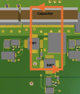
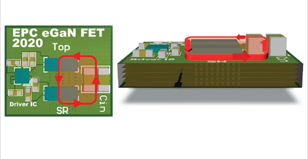
1. Minimize Parasitic Inductance in High-Speed Loops
GaN transistors operate at much higher switching frequencies than traditional silicon-based MOSFETs. As a result, parasitic inductance in power loops can cause significant voltage spikes, leading to efficiency losses and potential device failure.
Key Strategies:
- Keep high-current loops as small as possible by placing input capacitors close to the GaN FET.
- Use low-inductance capacitor arrays (e.g., MLCCs in parallel) to reduce loop inductance.
- Optimize power plane and return path to minimize loop area.
2. Optimize Thermal Management
GaN devices generate significant heat, especially in high-power applications. Effective thermal dissipation is critical to maintaining performance and reliability.
Key Strategies:
- Use thermal vias under GaN FETs to conduct heat to inner or bottom layers.
- Implement copper pours connected to the device’s thermal pad.
- Consider metal-core PCBs (e.g., aluminum or copper substrates) for high-power designs.
- Use thermal simulation tools to identify hotspots early in the design phase.
3. Reduce EMI with Proper Grounding
High-frequency switching in GaN circuits can generate electromagnetic interference (EMI), which may affect nearby components. Proper grounding techniques are essential.
Key Strategies:
- Use a solid ground plane to provide a low-impedance return path.
- Avoid split ground planes in high-frequency sections.
- Implement shielded traces for sensitive signals.
- Place decoupling capacitors strategically to suppress high-frequency noise.
4. Optimize Gate Drive Layout
The gate drive circuit is critical for GaN FET performance. Poor layout can lead to excessive ringing, increased switching losses, or even device failure.
Key Strategies:
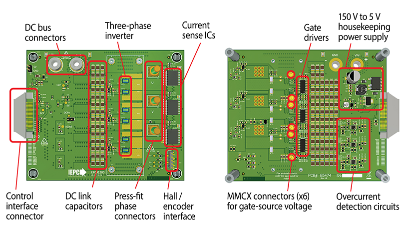
- Keep gate drive traces short and direct to minimize inductance.
- Use twisted-pair or shielded cables for external gate drive connections.
- Implement Kelvin connections for accurate gate voltage sensing.
- Add small gate resistors to dampen oscillations.
5. Use High-Frequency PCB Materials
Standard FR4 may not be sufficient for GaN circuits due to dielectric losses at high frequencies.
Key Strategies:
- Consider high-frequency laminates (e.g., Rogers, Isola, or Teflon-based materials).
- Optimize dielectric thickness to reduce parasitic capacitance.
- Ensure consistent impedance control for high-speed signals.
6. Implement Proper Power Plane Design
The power delivery network (PDN) must provide stable voltage with minimal impedance.
Key Strategies:
- Use multiple power planes for different voltage levels.
- Implement low-ESR/ESL capacitors near power pins.
- Avoid thin power traces that increase resistance.
7. Minimize Crosstalk Between High-Speed Signals
High-speed switching can induce crosstalk between adjacent traces, degrading signal integrity.
Key Strategies:
- Maintain adequate spacing between high-speed traces.
- Use differential pairs for sensitive signals.
- Route critical signals on different layers with ground shielding.
8. Optimize Layout for High-Frequency Switching
GaN’s fast switching requires careful attention to signal integrity and timing.
Key Strategies:
- Match trace lengths for synchronous signals.
- Avoid sharp bends in high-speed traces (use 45° or curved traces).
- Use simulation tools to analyze signal reflections and delays.
9. Ensure Robust ESD Protection
GaN devices are sensitive to electrostatic discharge (ESD), requiring proper protection.
Key Strategies:
- Place TVS diodes near sensitive inputs.
- Follow ESD-safe handling procedures during assembly.
- Use guard rings around high-impedance nodes.
10. Perform Extensive Testing and Validation
Before finalizing the PCB, prototype testing is crucial to validate performance.
Key Strategies:
- Use oscilloscopes with high-bandwidth probes to measure switching waveforms.
- Conduct thermal imaging to verify heat dissipation.
- Perform EMI compliance testing to ensure regulatory standards are met.
Conclusion
Designing PCBs for GaN-based applications requires careful consideration of high-frequency operation, thermal management, and signal integrity. By following these 10 optimization strategies, engineers can maximize efficiency, reliability, and performance in GaN power electronics.
Implementing minimized parasitic inductance, optimized thermal dissipation, and robust EMI control will ensure that GaN circuits operate at their full potential. As GaN technology continues to evolve, staying updated with advanced PCB design techniques will be key to unlocking its benefits in next-generation power systems.
This article provides a comprehensive guide for engineers working on GaN-based PCB designs, covering essential optimization techniques for improved performance and reliability. Would you like any sections expanded or additional details on specific topics?