
Trimming Excess PCB Material: Techniques and Best Practices
Introduction
Printed Circuit Boards (PCBs) are essential components in modern electronics, providing the foundation for mounting and interconnecting electronic components. During the manufacturing process, PCBs are often produced in panels containing multiple boards to optimize production efficiency. After assembly, these panels must be separated into individual PCBs, and any excess material must be trimmed to ensure proper fit and functionality.
Trimming excess PCB material is a critical step in PCB fabrication and assembly, as improper handling can lead to board damage, electrical issues, or mechanical instability. This article explores various techniques for trimming PCB excess material, best practices, and considerations to ensure a clean and precise finish.
Why Trim Excess PCB Material?
Before diving into the trimming methods, it’s important to understand why removing excess PCB material is necessary:
- Form Factor Compliance – Many PCBs are designed to fit into specific enclosures or slots, requiring precise dimensions.
- Aesthetic and Professional Finish – Excess material can make the PCB look unprofessional and may interfere with assembly.
- Improved Functionality – Removing unnecessary sections reduces weight and avoids potential electrical interference.
- Safety Considerations – Sharp edges or protruding material can pose risks during handling or installation.
Common Techniques for Trimming PCBs
Several methods are used to remove excess PCB material, each with its advantages and limitations. The choice of technique depends on factors such as board thickness, material type, required precision, and available tools.
1. Manual Cutting with Shears or Nibblers
- Best for: Thin PCBs (≤1.6mm), prototyping, low-volume production.
- Tools: PCB shear, nibbler, or heavy-duty scissors.
- Process: The excess material is manually cut along the outline using shears or nibblers.
- Pros:
- Low-cost and accessible for hobbyists.
- No specialized machinery required.
- Cons:
- Prone to uneven edges and burrs.
- Not suitable for thick or rigid PCBs.
- Labor-intensive for large batches.
2. Scoring and Breaking (V-Groove Method)
- Best for: FR4 PCBs with predefined breakaway tabs or V-grooves.
- Tools: Scoring tool or a straight edge and pressure.
- Process:
- The manufacturer pre-cuts V-shaped grooves along the separation lines.
- The board is then snapped along these grooves.
- Pros:
- Fast and cost-effective for mass production.
- Minimal tooling required.
- Cons:
- Can leave rough edges requiring additional sanding.
- Risk of cracking if not done carefully.
3. CNC Routing/Milling
- Best for: High-precision cuts, complex shapes, and rigid PCBs.
- Tools: CNC router or milling machine with a PCB-specific bit.
- Process:
- The PCB is secured on the CNC bed.
- A programmed path guides the router to cut along the desired outline.
- Pros:
- Highly precise and repeatable.
- Can handle intricate designs and curves.
- Cons:
- Expensive equipment required.
- Slower than other methods for simple cuts.
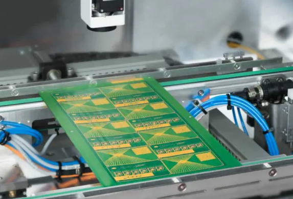
4. Laser Cutting
- Best for: Thin PCBs, flexible circuits, and high-precision applications.
- Tools: CO₂ or fiber laser cutter.
- Process:
- A laser beam vaporizes the excess material along the cutting path.
- Pros:
- Extremely precise with clean edges.
- No physical contact reduces mechanical stress.
- Cons:
- High equipment cost.
- May produce toxic fumes (requires ventilation).
5. Punching (Die Cutting)
- Best for: High-volume production of standardized PCB shapes.
- Tools: Hydraulic punch press with a custom die.
- Process:
- A die is pressed into the PCB to punch out the excess.
- Pros:
- Extremely fast for mass production.
- Consistent results with minimal post-processing.
- Cons:
- High initial cost for custom dies.
- Limited to predefined shapes.
Best Practices for Trimming PCBs
Regardless of the chosen method, following best practices ensures a clean and safe trimming process:
1. Verify Design Files Before Cutting
- Ensure the Gerber files or CAD designs include proper cut lines and tolerances.
- Double-check dimensions to avoid cutting into functional areas.
2. Use Proper Safety Gear
- Wear safety glasses when cutting or milling PCBs to protect against flying debris.
- Use gloves when handling sharp edges.
3. Deburr and Smooth Edges
- After cutting, use fine-grit sandpaper or a deburring tool to remove rough edges.
- This prevents copper traces from peeling and improves aesthetics.
4. Secure the PCB During Cutting
- Clamp the PCB firmly to prevent movement, which can lead to jagged cuts.
- For CNC or laser cutting, use vacuum beds or adhesive mats for stability.
5. Minimize Stress on the Board
- Avoid excessive force when snapping PCBs to prevent microcracks.
- For sensitive components, consider supporting the board during cutting.
6. Inspect for Damage After Trimming
- Check for delamination, cracked traces, or lifted pads.
- Use a magnifying glass or microscope for fine inspections.
Post-Trimming Considerations
Once the excess material is removed, additional steps may be necessary:
- Cleaning – Remove dust and debris from cutting using compressed air or isopropyl alcohol.
- Edge Plating (If Required) – Some high-frequency or ruggedized PCBs require plated edges for shielding or mechanical strength.
- Conformal Coating – Apply protective coating if the trimmed edges expose sensitive areas to moisture or contaminants.
Conclusion
Trimming excess PCB material is a crucial step in PCB manufacturing and assembly, affecting both functionality and aesthetics. The choice of trimming method depends on factors such as precision requirements, production volume, and available tools. Whether using manual cutting, CNC routing, laser cutting, or die punching, adhering to best practices ensures clean, safe, and reliable results.
By understanding the different techniques and their applications, engineers and manufacturers can optimize their PCB trimming processes for efficiency and quality. Properly trimmed PCBs not only fit better in their intended applications but also exhibit improved durability and performance.
Final Thoughts
As PCB technology evolves with thinner, more complex designs, trimming methods will continue to advance. Automation and laser-based techniques are becoming more prevalent, offering faster and more precise solutions. Staying updated with these developments ensures that PCB trimming remains an efficient and reliable process in electronics manufacturing.