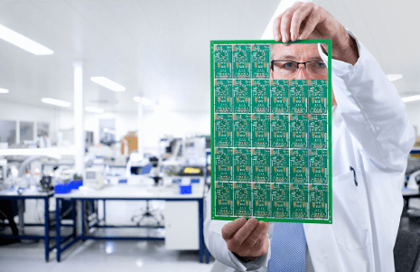
PCB Panel Design Tips
In the electronics manufacturing industry, PCB (printed circuit board) panel design is a key factor affecting board utilization and production costs. Efficient panel design not only reduces material waste but also improves production efficiency. This article will focus on several practical PCB panel design techniques to help you effectively improve board utilization.
1.Planning the Panel Layout
Dense Arrangement: During the initial design phase, circuit components should be arranged as closely as possible to minimize blank areas. You can use the CAD software’s automatic layout function to optimize the minimum spacing between components through algorithms.
Modular Design: Design identical or similar circuit modules to standard sizes to facilitate reuse across projects, reducing design time and errors.
Symmetrical Layout: Strive for a symmetrical panel layout. This not only helps reduce deformation during processing but also improves panel utilization.
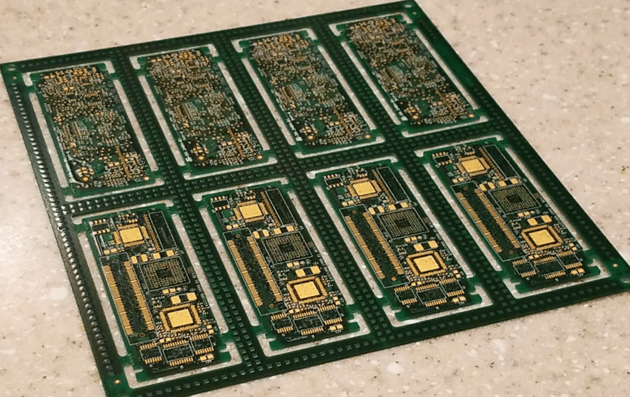
2.Choosing the Appropriate Panelization Method
V-Cut Panelization: Suitable for larger, regularly shaped PCBs. V-grooving allows for quick separation of individual components, improving production efficiency.
Stamp Hole Panelization: Suitable for smaller, high-density PCBs. The stamp hole connection method facilitates subsequent processing and separation while maintaining high board utilization.
Mixed Panelization: PCBs of different sizes and shapes are mixed together to maximize board space. This method requires precise calculation and layout to avoid waste.
3.Utilizing Automated Design Tools
CAD Software Optimization: Use advanced CAD software for panel design, leveraging its built-in optimization algorithms to automatically adjust the layout and improve board utilization.
3D Simulation: Preview the panelization results through 3D simulation technology to promptly identify and resolve potential issues such as component interference and circuit conflicts.
Parametric Design: Utilize parametric design methods to quickly adjust panel parameters based on project requirements, achieving efficient design.
4.Consider Processing Requirements
Leave Processing Margins: When designing the panelization, leave ample processing margins to facilitate subsequent cutting, drilling, and other processes.
Avoid Slender Strip Designs: Slender PCB strips are prone to deformation during processing; design them to a more stable shape.
Optimize Hole Layout: Arrange holes rationally to avoid excessively concentrated holes, which can reduce board strength.
5. Other Practical Tips
Overlapping Design: For certain small components or circuit modules, consider overlapping to save space.
Multilayer Design: By effectively utilizing multilayer design, circuits with different functions can be stacked together to improve space utilization.
Customized Tools: Develop customized panel design tools based on your needs to improve design efficiency and accuracy.
By rationally planning the panel layout, selecting the appropriate panelization method, utilizing automated design tools, and considering processing requirements, you can significantly increase PCB board utilization. These practical tips not only help reduce production costs but also improve product quality and production efficiency.
Shenzhen Ying Chuangli Electronics Co., Ltd., established in 2004, specializes in one-stop services including circuit board production, component procurement, SMT processing, assembly and testing. We position ourselves as a “professional and fast, high-variety, low-volume, one-stop EMS service provider.” We are equipped with high-precision imported equipment, including fully automatic multi-function placement machines, reflow soldering, wave soldering, selective wave soldering, X-ray inspection machines, and AOI equipment. Our products have passed UL safety certification, ISO13485 medical device quality management system certification, ISO9001 international quality system certification, and IATF16949 international automotive electronics quality system certification. Our products are used in many fields such as automotive electronics, medical equipment, industrial control, aerospace, and communication equipment.