The”Heart”and”Nerves”of Mobile phones and Computers:Unveiling the Secrets of the PCB
When we marvel at the ultra-thin design of mobile phones and immerse ourselves in the blazing-fast performance of computers,we often see the dazzling screen and exquisite,integrated bodies.But the unassuming”hero”behind all this life and vitality lies within:the PCB is the“neural network”and “skeletal blood vessels”that permeate the entire body,transmitting all commands and energy.
1.What is a PCB?The”urban infrastructure”of the Electronics world
Imagine a modern metropolies:skyscrapers(chip components)stand tall,but what keeps the city running is a complex yet well-organized underground network of subways,roads,and power grids.The PCB is a miniature version of this”urban infrastructure”
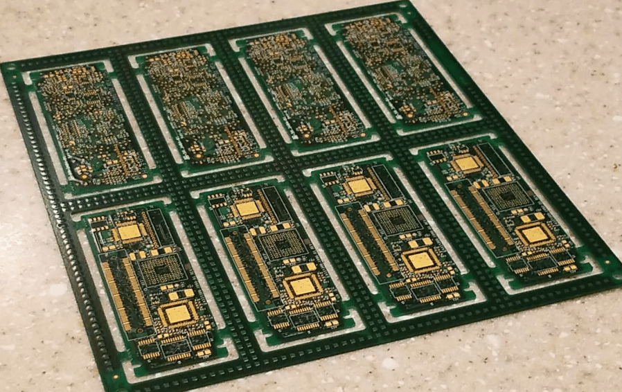
It’s typically a green(or sometime black,blue,etc)insualting board,covered in fine copper wire(circuits)and countless drilled hole(vias).These copper wires are the”roads”,precisely transmitting data signals and electrical energy.Chips,resistors ,capacitors,and other electronic compoents,large and small,are the”functional buildings”nestled along these roads and at their intersections,The core mission of the PCB is to connect all these electronic component together in the most efficient and reliable way possible,forming an organic whole work together.
2.How Do the “Heart “and”Nerves”work Together?
The”Heart’s Location”:The central processing unit(CPU),Often referred to as the”heart” of a mobile phone or computer,and other core chips(such as the GPU and other core chips(Such as the CPU memory),cannot function independently.They are precisely soldered to specific locations on the PCB.The PCB provide this “heart”with a stable power supply(like blood) and high-speed data channels(like main nerve arteries),enabling it to retrieve instructions from memory and issue commands to various components.
“The Nerves”Transmission:The circuits on the PCB are the device‘s neural network When you touch the screen,this command,like a nerve impulse,travels through the circuits on the PCB,from the touch chip to the CPU”brain”,After processing,the “brain”then transmits the command””display this image”through another set of circuits to the dispaly chip and screen,ALL of this happens in a billion of a second,via the hair-thin”nerves”on the PCB.A break or short circuit in any one of these “nerves”can cause device malfunction or even paralysis.

3.PCB Design and Manufacturing:A precise Art and Science
Designing and manufacturing a high-performance PCB is an extremely challenge task,especially in today’s pursuit of thinness and compactness.
Design:The Urban Planning Map of the Electronic World
Electronic world
Engineers use specialized software to perform layout and routing,which is like creating an ultra-precise urban traffic map.They need to ensure:
Signal Integrity:High-speed signals are like sports cars on a highway;they can’t have too many sharp turns and interference,otherwise the data will be “erroneous”.
Power Integrity:Ensuring that the voltage reaching each chip is stable and pure,just like ensuring adequate water pressure in every household.
Electromagnectic compatibility:Prevents signals on different “paths”from interfering with each other ,preventing crosstalk within the device or affecting external devices.
”Heat dissipation design”:Plans heat dissipation pathways for heat-generating chips(such as the CPU) to prevent overheating.
“Manufacturing:Micron-level engraving techniques”
The PCB manufacturing process integrates chemical,optical,and precision mechanical techniques,Through processes such as exposure and etching,the designed circuit is”engraved”into the copper-clad laminate.Drilling and electroplating create”overpasses”between the upper and lower layers. Finally,components are attached and soldered,and a complete”electronic city”is born.
4.From Simplicity to Sophistication:The Evolution of PCB Technology
PCB technology continues to evolve to meet more demanding requirement:
“Multilayer boards”:Modern mobile phone motherboard may have more than 10 layers,like overpasses and underground tunnels,greatly improving wiring density and signal quality.
HDI(High Density Interconnect) Technology:Using finer line widths and smaller holes.mobile phones can achieve more powerful functions in a smaller space.
Flexible printed Circuit(FPC):Bendable like paper,it is widely used in mobile phones’foldable screen,camera modules,and other applications requiring flexible connections.It is a flexible extension of the “neural network”.
Conclusion
Next time you pick up your phone or turn on your computer,imagine that beneath the cold exterior,a vibrant and dynamic microcosm of PCBs is operating at high speed.Though invisible,it is the physical foundation of all intelligence and functionality .This sophisticated”neural network”silently carries a torrent of information,driving every interaction we have with the digital world. It is not only a culmination of technology but also the silent yet powerful pulse of modern civilization.