What is HDI PCB? A Complete Beginner Guide
The global HDI PCB market surpassed $14 billion in 2023 and is projected to grow at roughly 7% CAGR through 2030, according to research from Mordor Intelligence — a clear signal that high-density interconnect technology is no longer a niche specialty but the backbone of modern electronics. An HDI PCB (High Density Interconnect Printed Circuit Board) is a circuit board engineered with finer lines, smaller vias, and higher wiring density than conventional PCBs, enabling more functionality in a dramatically smaller footprint. If you’ve ever wondered how smartphones, medical implants, or aerospace avionics pack so much computing power into such compact packages, HDI technology is the short answer.
This guide breaks down everything a beginner needs to know — from the fundamental structure of an HDI PCB and how it differs from standard boards, to real-world applications, design trade-offs, and the decision framework for choosing the right stackup configuration for your project.
What Is an HDI PCB and What Does HDI Stand For
HDI stands for High Density Interconnect. An HDI PCB is a printed circuit board engineered with finer lines, smaller spaces, and tinier vias than conventional boards — allowing significantly more components and routing channels per unit area. Think of it as packing a highway system into the footprint of a neighborhood street.
Quick definition: A High Density Interconnect PCB is any board that uses microvias (≤150 µm diameter), fine lines/spaces (≤75 µm), and high-density connection pads to achieve greater wiring density than traditional PCB fabrication allows.
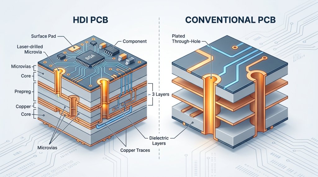
What actually separates HDI from a standard FR-4 board? Three things: microvia technology, build-up lamination structures, and advanced materials. Conventional boards rely on mechanically drilled through-holes — typically 200–300 µm or larger. HDI boards use laser-drilled microvias as small as 75 µm, which frees up routing space on inner layers and dramatically reduces board size.
The IPC-2226 standard, published by the Association Connecting Electronics Industries (IPC), formally classifies HDI structures into six types based on microvia layer count and configuration. Most designs you’ll encounter fall into Type I (single build-up layer) or Type II (two or more build-up layers with stacked or staggered microvias).
Why does this matter practically? A smartphone motherboard, for example, would be physically impossible to manufacture using conventional PCB methods. The density requirements demand 8–12 layers of HDI construction with line widths under 50 µm. If you’re sourcing boards for compact, high-performance electronics, working with a proven HDI PCB manufacturer is essential to achieving reliable results at these tolerances.
How HDI PCB Technology Evolved and Why It Matters Today
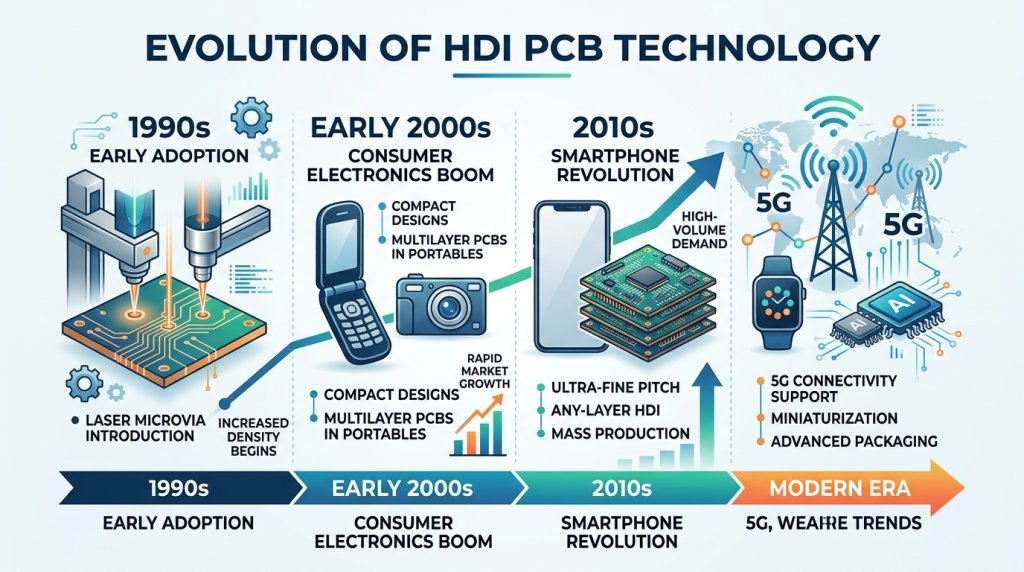
The roots of high density interconnect technology trace back to the mid-1990s, when Japanese manufacturers — notably Ibiden and Shinko Electric — pioneered microvia drilling using laser ablation instead of mechanical bits. Before that breakthrough, multilayer boards relied entirely on through-hole vias that consumed valuable routing space. The shift to laser-drilled microvias (under 150 µm in diameter) unlocked a new era: designers could stack more layers into thinner profiles without sacrificing electrical performance.
By the early 2000s, HDI PCB fabrication had moved from niche telecom applications into mainstream consumer electronics. Apple’s adoption of any-layer HDI construction for the iPhone mainboard around 2007 signaled a turning point. Suddenly, every smartphone OEM needed the same capability, and fabrication volumes surged.
According to a Prismark Partners report, the global HDI PCB market exceeded $12 billion in annual revenue by 2023, growing at roughly 7–9% CAGR — outpacing the broader PCB industry average of about 4%.
Three forces are accelerating adoption right now:
- Device miniaturization: Smartwatches, TWS earbuds, and implantable medical devices demand board thicknesses below 0.4 mm with 50 µm line/space routing.
- 5G infrastructure: Massive MIMO antenna modules and mmWave front-end modules require controlled-impedance microvias at 28 GHz and above, where signal integrity tolerances are razor-thin.
- Automotive electrification: ADAS radar units and EV battery management systems pack hundreds of components into compact enclosures, making high density interconnect designs essential.
Choosing a reliable HDI PCB manufacturer has become a strategic decision, not just a procurement checkbox. The technology is no longer a premium option — it’s the baseline for any product competing on size, speed, or power efficiency.
Key Differences Between HDI and Standard Circuit Boards
Strip away the marketing language and the core distinction is straightforward: an HDI PCB packs more connections into less space. But “more density” barely scratches the surface. The engineering gaps between HDI and conventional boards show up in trace geometry, via architecture, layer economics, and signal behavior — all of which affect cost, performance, and design freedom.
Where the Specs Diverge
Standard PCBs typically use through-hole vias with diameters of 0.3 mm or larger and trace widths around 150–200 µm. HDI boards push trace/space down to 50–75 µm and rely on laser-drilled microvias as small as 75–100 µm. That single change — shrinking the via — cascades into everything else: tighter routing channels, fewer required layers, and thinner overall stackups.
A conventional 12-layer board can often be replaced by an 8-layer HDI design with equivalent or better routing capacity. Fewer layers mean less material, shorter drill cycles, and reduced weight — critical factors for any HDI PCB manufacturer optimizing production yield.
| Parameter | Standard PCB | HDI PCB |
|---|---|---|
| Minimum Trace/Space | 150–200 µm | 50–75 µm |
| Via Type | Mechanical through-hole | Laser-drilled microvias, blind & buried vias |
| Via Diameter | ≥ 0.3 mm | 0.075–0.15 mm |
| Typical Layer Count | 4–16 layers | 4–20+ layers (fewer needed for same routing) |
| Board Thickness | 1.2–2.4 mm | 0.4–1.2 mm |
| Routing Density | Moderate | 2–3× higher per unit area |
| Signal Integrity | Adequate for low-to-mid frequency | Superior — shorter paths, reduced stubs |
| Pad Density (BGA Escape) | Limited to dog-bone fanout | Via-in-pad enables full-array BGA routing |
Why This Matters in Practice
Shorter signal paths directly reduce parasitic inductance and capacitance. According to IPC-2226 — the industry standard governing HDI design — these improvements translate to measurable gains in high-speed signal integrity, particularly above 1 GHz. That’s not a theoretical benefit; it’s the reason smartphones, medical implants, and aerospace avionics all demand HDI construction.
Rule of thumb: if your design requires BGA packages with pitch below 0.8 mm, standard through-hole technology simply cannot route the escape pattern. HDI isn’t optional at that point — it’s mandatory.
Understanding HDI Structures — Microvias, Blind Vias, and Buried Vias
Three structural elements separate an HDI PCB from a conventional board: microvias, blind vias, and buried vias. Understanding how each one works — and how they combine — is essential before you touch a stackup diagram.
Microvias: The Foundation of HDI Routing
A microvia is any plated hole with a diameter of 150 µm (6 mil) or less and a depth-to-diameter aspect ratio no greater than 1:1, per IPC-2226 standards. These tiny interconnects are formed by UV or CO₂ laser drilling, which ablates dielectric material one layer at a time with positional accuracy under ±25 µm. Mechanical drilling simply cannot achieve this — conventional drill bits bottom out around 200 µm and generate too much heat for ultra-thin dielectrics.
Why does the size matter so much? A 100 µm microvia occupies roughly one-tenth the pad area of a standard 300 µm through-hole via. That freed-up real estate translates directly into more routing channels per layer.
Blind Vias and Buried Vias
- Blind vias connect an outer layer to one or more inner layers without penetrating the entire board. They’re visible from one side only — hence “blind.”
- Buried vias sit entirely within the internal layers, invisible from either surface. They link inner layers to each other and free up valuable outer-layer space for component pads.
Both types reduce the total number of through-holes competing for routing space, which is why any reputable HDI PCB manufacturer relies heavily on these configurations.
Stacked vs. Staggered Via Arrangements
| Arrangement | Description | Best For |
|---|---|---|
| Stacked | Microvias aligned directly on top of each other, copper-filled for structural integrity | BGA breakout with ≤0.5 mm pitch; maximum vertical density |
| Staggered | Microvias offset layer-to-layer, reducing stress concentration | Cost-sensitive designs where moderate density is sufficient |
Stacked vias demand copper filling and planarization — adding roughly 15–20% to fabrication cost — but they enable direct vertical connections across three or more layers. Staggered vias are more forgiving during lamination and cost less, yet they consume slightly more lateral space because of the offset.
Rule of thumb: if your BGA pitch is 0.4 mm or tighter, stacked microvias are practically mandatory. Above 0.65 mm, staggered arrangements usually suffice.
HDI PCB Stackup Types and Build-Up Configurations
Stackup classification tells you exactly how many microvia layers sit on each side of the core. The notation is simple: the numbers before and after “N” represent build-up layers, while N is the conventional core layer count. Getting this right determines routing density, signal integrity, and — critically — your budget.
1+N+1: The Entry Point
One build-up layer on each side of the core. A single laser-drilled microvia layer connects the outer copper to the next layer down. This configuration handles most smartphone accessories, wearables, and mid-complexity IoT devices. Cost premium over standard boards? Roughly 20–30%, making it the most accessible HDI option.
2+N+2: The Mid-Range Workhorse
Two sequential build-up layers per side, with stacked or staggered microvias. Designers gain significantly more routing channels — ideal for BGA packages with 0.5 mm pitch or tighter. Signal integrity improves because shorter via stubs reduce impedance discontinuities. Expect fabrication costs to jump another 25–40% above 1+N+1.
3+N+3 and Beyond
Three build-up layers per side push into premium territory. Stacked microvias here require copper-filled processes to maintain structural reliability through multiple lamination cycles. Applications include advanced networking equipment and high-performance computing modules where layer count reduction matters.
ELIC / Any-Layer HDI
Every Layer Interconnect (ELIC) eliminates the traditional core entirely. Every copper layer connects to every adjacent layer through copper-filled stacked microvias, enabling maximum routing freedom. Apple’s iPhone logic boards famously use any-layer HDI PCB designs — sometimes packing 10+ layers into a board thinner than 1 mm. The tradeoff is clear: manufacturing complexity and cost are the highest of any build-up type.
Rule of thumb from IPC-2226 guidelines: choose the lowest build-up level that satisfies your routing and component density requirements. Over-specifying stackup inflates cost without functional benefit.
If you need guidance matching a stackup to your project, working with an experienced HDI PCB manufacturer early in the design phase prevents costly respins later.
The Main Advantages of High Density Interconnect Technology
Why do engineers consistently choose HDI over conventional boards for space-constrained, high-performance designs? The answer isn’t a single benefit — it’s a cascade of interconnected gains that compound once you shrink trace widths below 75 µm and swap through-hole vias for microvias.
Dramatic Size and Weight Reduction
A single HDI PCB can replace a conventional 8-layer board with a 4- or 6-layer stackup while maintaining equivalent routing capacity. That translates to 40–60% less board area in many designs, according to IPC research on high density interconnect adoption. For wearable medical devices and smartphones, shaving even 0.3 mm off total thickness directly enables slimmer product enclosures and lighter shipping weight.
Superior Signal Integrity and Electrical Performance
Shorter signal paths mean lower parasitic inductance and capacitance. Microvias with aspect ratios under 1:1 produce stub lengths so small they’re electrically negligible at frequencies up to 25 GHz. The result? Cleaner eye diagrams, fewer signal reflections, and reduced electromagnetic interference — critical for DDR5 memory routing and 5G RF front-end modules.
Improved Thermal Management and Reliability
Copper-filled microvias act as efficient thermal conduits, pulling heat away from BGA pads directly through the board. This localized heat dissipation can lower junction temperatures by 10–15°C compared to designs relying on thermal vias with larger diameters and air gaps. Fewer mechanical drill holes also means less structural stress, which boosts long-term solder joint reliability under thermal cycling — a key concern in automotive electronics rated for –40°C to +150°C operation.
Higher Component Density Per Unit Area
- Pad-in-via (via-in-pad) designs eliminate fanout space, allowing 0.4 mm pitch BGAs that would be unroutable on standard boards.
- Both-side component placement becomes practical because blind and buried vias free up surface real estate.
- Designers working with a capable HDI PCB manufacturer can achieve component densities exceeding 30 parts per cm², roughly double what conventional technology supports.
The real competitive edge of HDI isn’t any single metric — it’s the ability to simultaneously improve electrical performance, shrink the footprint, and increase reliability without trading one against the other.
Common Applications and Industries That Rely on HDI PCBs
Smartphones are the single largest consumer of HDI technology. Apple’s iPhone mainboards pack over 1,000 components into a space smaller than a credit card — impossible without stacked microvias and 50µm trace widths. Every flagship Android device from Samsung, Xiaomi, and Google follows the same playbook.
Medical devices demand miniaturization with zero margin for failure. Implantable cardiac defibrillators, cochlear implants, and endoscopic cameras all rely on HDI PCB designs to shrink board footprints while maintaining signal integrity inside the human body. The shorter signal paths reduce electromagnetic interference, which is critical when a device sits millimeters from living tissue.
Where else does high density interconnect technology prove indispensable?
- Automotive ADAS: LiDAR modules, radar sensors, and camera ECUs in systems from Mobileye and Continental require multi-layer HDI boards that survive -40°C to +125°C thermal cycling while processing gigabits of sensor data per second.
- Aerospace avionics: Flight control computers and satellite communication units benefit from the 40-60% weight reduction HDI offers over conventional boards — every gram matters at $10,000+ per kilogram to orbit.
- IoT sensors: Wearables and industrial edge devices need boards as small as 8mm × 8mm. Only HDI stackups can route the necessary power and data lines in that footprint.
- Military electronics: Encrypted communication modules and missile guidance systems use any-layer HDI for maximum routing density inside ruggedized, shock-resistant enclosures.
The common thread across all these sectors is the same: tight space, high reliability, and complex routing that conventional boards simply cannot deliver. For demanding projects in any of these fields, partnering with a trusted HDI PCB manufacturer like Andwin PCB ensures your design meets both performance specs and volume production requirements.
When Should You Choose an HDI PCB for Your Project
Not every design needs HDI. A two-layer board running a simple sensor module? Standard FR-4 handles that fine at a fraction of the cost. The real question is where the tipping point lies — the moment conventional routing can no longer meet your electrical, mechanical, or thermal requirements.
BGA Pitch Is Your First Decision Trigger
If your design includes BGAs with a pitch of 0.65 mm or finer, standard through-hole vias physically cannot fan out between pads. At 0.5 mm pitch — common on application processors from Qualcomm and MediaTek — you need microvias and pad-in-via technology. There is no workaround. Below 0.4 mm pitch, you’re likely looking at 2+N+2 or 3+N+3 stackups to escape all signal rows cleanly.
Size Constraints and Layer Count Pressure
When your enclosure shrinks but component count stays the same, an HDI PCB lets you consolidate routing into fewer layers. A design that requires 12 standard layers might drop to 8 layers with a 1+N+1 build-up — saving 15–25% on total board thickness. Wearables, earbuds, and medical implants almost always hit this threshold.
Cost-Benefit Reality Check
Rule of thumb: HDI adds 20–40% to bare board fabrication cost for a 1+N+1 structure. That premium climbs to 60–100%+ for 3+N+3 builds. Weigh this against savings from reduced layer count, smaller board area, and fewer assembly defects.
For production volumes above 5,000 units, the per-unit cost difference narrows significantly because panel utilization improves with smaller boards. Prototyping, however, stings — expect 3–5 week lead times from most fabricators versus 1–2 weeks for standard multilayer.
Quick Decision Checklist
- BGA pitch ≤ 0.65 mm: HDI required
- Board area reduction > 30% needed: HDI strongly recommended
- Signal integrity targets demand shorter trace lengths: HDI beneficial
- Budget-constrained prototype with relaxed size limits: stick with standard multilayer
- Flex requirements with tight bend radii: consider rigid-flex before HDI
If you’re crossing two or more of those thresholds simultaneously, partner with an experienced HDI PCB manufacturer early in the schematic phase. Stackup decisions made after layout begins almost always result in costly respins.
Design and Manufacturing Challenges to Consider with HDI PCBs
Tighter geometries demand tighter discipline. Trace widths on HDI boards routinely drop below 75 µm (3 mil), and microvia land pads shrink to 250 µm — tolerances that leave almost zero room for registration drift or etching variation. A design rule set that works fine on a standard 6-mil trace/space board will cause opens and shorts the moment you push into HDI territory.
Cost and Lead Time Realities
Expect fabrication costs 30–80% higher than conventional multilayer boards, depending on the stackup complexity. Each sequential lamination cycle adds processing time, and laser drilling microvias is slower than mechanical drilling through-holes. A 2+N+2 build might carry a 3–4 week lead time; jump to 3+N+3 or any-layer, and you’re looking at 5–7 weeks from most fabricators.
Material Selection Matters More Than You Think
Standard FR-4 prepreg can develop z-axis expansion problems during multiple lamination cycles. Low-CTE prepregs — such as Panasonic Megtron 6 or Isola IS415 — reduce the risk of microvia cracking caused by thermal stress. Skipping this material upgrade on a 3+N+3 stackup is a reliability gamble you’ll lose.
Expert Tips to Avoid Common Pitfalls
- Start DFM collaboration early. Share your stackup concept with your HDI PCB manufacturer before routing begins — not after Gerber export.
- Use stacked microvias only when necessary. Staggered vias are cheaper and more reliable for most 2+N+2 designs.
- Define aspect ratios explicitly. Keep microvia depth-to-diameter ratios at or below 0.75:1 to maintain plating reliability, per IPC-2226 guidelines.
- Run impedance simulations on the actual stackup. Dielectric thickness variations in thin cores (50–75 µm) shift impedance more than engineers expect.
The single biggest HDI PCB failure mode isn’t a bad design — it’s a good design sent to the wrong fabricator without a DFM review. Align capabilities before committing.
Frequently Asked Questions About HDI PCBs
What is an HDI PCB in simple terms?
It’s a circuit board that packs more connections into less space by using laser-drilled microvias, finer traces, and thinner dielectrics. Think of it as the difference between a two-lane road and a multi-level highway — same footprint, far more capacity.
How many layers can an HDI board have?
Typical HDI PCB designs range from 4 to 20+ layers. Smartphones commonly use 8–12 layer stackups, while advanced networking equipment can push beyond 20 layers with “any-layer” interconnect structures where every layer contains microvias.
What is the minimum via size in HDI?
Laser-drilled microvias typically measure 75–150 µm (3–6 mil) in diameter. Some leading fabricators achieve 50 µm vias for cutting-edge applications, though 100 µm remains the production sweet spot for balancing yield and cost.
How much more does HDI cost than a standard PCB?
Expect a 30–80% premium for a 1+N+1 build-up over an equivalent-layer conventional board. Higher-order structures (2+N+2, 3+N+3) can double or triple the price. However, HDI often eliminates the need for extra layers entirely, which can offset the per-layer cost increase. A reliable HDI PCB manufacturer can help you optimize the stackup to control expenses.
Is HDI necessary for all high-speed designs?
No. Plenty of high-speed boards — 10 Gbps Ethernet switches, for example — work fine on standard through-hole technology with careful impedance control. HDI becomes essential when component pitch drops below 0.5 mm, when BGA escape routing demands microvias, or when signal integrity requirements and board size constraints collide. If your design doesn’t face those pressures, conventional fabrication is the smarter financial choice.
Summary — Choosing the Right HDI Solution for Your Next Design
High density interconnect technology isn’t a universal upgrade — it’s a precision tool. The right moment to reach for it is when your design demands finer pitch components, shorter signal paths, or a smaller form factor that conventional through-hole boards simply cannot deliver.
Here’s what matters most from everything covered above:
- Microvias, blind vias, and buried vias are the structural backbone of HDI. Understanding the difference between a 1+N+1 and a 3+N+3 stackup directly affects your cost, lead time, and electrical performance.
- Signal integrity gains are real and measurable. Shorter interconnect lengths reduce parasitic inductance and capacitance, which matters enormously at data rates above 5 Gbps.
- Cost scales with complexity. A simple 1+N+1 build adds roughly 30–40% over a standard multilayer board, while any-layer designs can double or triple that figure. Match the stackup to the actual routing challenge — don’t over-specify.
- Manufacturer capability is the bottleneck. Not every fabricator can hold 75 µm laser-drilled microvias or 50 µm trace/space with acceptable yield. Vet your supplier early.
One decision separates successful HDI projects from costly redesigns: engaging your fabricator before you finalize the stackup. DFM feedback at the schematic stage catches issues that become expensive at prototyping.
If your next product targets smartphones, wearables, medical implants, or high-speed networking, an HDI PCB is likely the shortest path to a compact, reliable design.
Ready to move forward? Reach out to an experienced HDI PCB manufacturer who can review your Gerber files, recommend the optimal stackup type, and provide a realistic cost-to-performance assessment tailored to your specific application. That single conversation often saves weeks of iteration down the line.