What Is HDI PCB? Complete Beginner Guide
HDI PCB (High Density Interconnect Printed Circuit Board) technology has transformed how modern electronics are designed and manufactured. As smartphones get thinner, cars get smarter, and medical devices become more portable, engineers need circuit boards that pack more functionality into less space. That’s where HDI PCB comes in — a manufacturing breakthrough that uses laser-drilled microvias, fine-line traces, and sequential lamination to achieve wiring densities that traditional PCBs simply cannot match. Whether you’re an electronics engineer evaluating your next board design or a procurement specialist researching manufacturing options, this guide will walk you through everything you need to know about HDI PCB – High Density Interconnect PCB technology.
Quick Answer: HDI PCB is an advanced circuit board technology using laser-drilled microvias (≤150µm) and fine lines/spaces (≤75µm) to achieve higher wiring density per unit area than conventional through-hole PCBs, enabling smaller, lighter, and higher-performance electronic devices.
The Problem: Why Traditional PCBs Fall Short
The Miniaturization Challenge
Modern electronics face an unprecedented challenge: consumers demand devices that are simultaneously smaller, faster, and more powerful. Traditional through-hole PCBs, with mechanical drilled vias typically ≥0.3mm in diameter, create fundamental physical barriers to achieving the component densities required by today’s high-pin-count ICs.
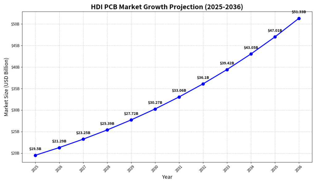
According to industry analysis from Future Market Insights, the HDI PCB – High Density Interconnect PCB market was valued at USD 19.50 billion in 2025 and is projected to reach USD 51.34 billion by 2036, growing at a CAGR of 9.20%. This explosive growth directly reflects the limitations of conventional PCB technology in addressing modern design requirements.
Key Pain Points Engineers Encounter
- Through-hole vias consume excessive routing space, forcing larger board sizes or additional layers that increase cost and weight
- Standard PCB technology cannot accommodate fine-pitch BGAs below 0.5mm pitch, limiting component selection for high-performance designs
- Signal integrity degrades as trace lengths increase to route around oversized vias, causing timing issues in high-speed applications
- Layer count inflation drives up material costs and manufacturing complexity, with some traditional designs requiring 20+ layers
- Thermal management becomes critical as dense component placement concentrates heat in confined areas
Industry Insight: Data reveals that per-vehicle PCB area increases by 5% to 8% with each new model year, with ADAS, infotainment, and battery management modules demanding interconnect densities that conventional through-hole PCBs fundamentally cannot achieve.
The Cost of Sticking with Old Technology
Engineers continuing to rely solely on traditional PCB methods face measurable consequences. Analysis shows that devices using conventional PCBs require 15% to 30% more board area to achieve equivalent functionality. In competitive markets like consumer electronics, where every millimeter matters, this translates directly to lost market share and reduced user satisfaction.
Consider this real-world scenario: a wearable fitness tracker design using conventional PCB technology requires a 4-layer, 25mm × 18mm board to accommodate the Bluetooth SoC, IMU sensors, and heart rate monitor. Switching to HDI PCB technology enables the same functionality on an 8-layer, 18mm × 12mm board — a 52% reduction in board area that directly enables a more comfortable form factor and longer battery life through the additional space gained for the battery cell.
HDI PCB Technology: How It Solves the Density Challenge
Defining HDI PCB Architecture
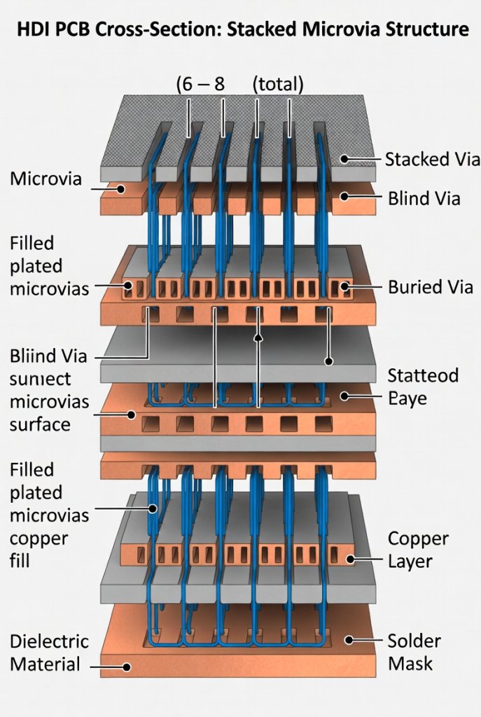
HDI PCB technology addresses these limitations through a fundamentally different approach to interconnection. Instead of relying solely on through-hole vias that penetrate the entire board thickness, HDI PCBs incorporate multi-layers of copper filled with stacked micro-vias — laser-drilled interconnects typically measuring ≤0.15mm (150µm) in diameter.
The defining characteristics of HDI PCB include:
- Laser-drilled microvias connecting adjacent layers with diameters as small as 0.004 inches (0.10mm)
- Fine lines and spaces below 75µm, enabling dense trace routing patterns
- Sequential lamination build-up allowing layer-by-layer construction for complex interconnect structures
- Stacked or staggered microvia configurations providing flexible routing solutions for high-pin-count devices
- Via-in-pad technology maximizing routing space beneath fine-pitch BGA components
Core Technical Advantages
Technical Note: Testing reveals that the combination of fine track and gap features with laser-drilled blind vias enables interconnection between PCB layers using the smallest pad diameter possible, creating design flexibility previously unattainable with mechanical drilling methods.
The performance improvements HDI PCB delivers are substantial:
- Dense trace routing — Fine-line capabilities enable more traces per layer, reducing total layer count
- Enhanced power stabilization — Shorter via paths reduce parasitic inductance and capacitance
- Reduced EMI effects — Compact routing minimizes antenna loops and signal radiation
- Improved signal integrity — Shorter interconnection paths support high-speed applications above 10Gbps
- Design efficiency — Decreased need to relocate components saves development iterations
- Space optimization — Increased available area for additional functionality within the same form factor
Microvia Structures: Stacked vs. Staggered
| Microvia Type | Structure | Reliability | Cost Factor | Best Application |
|---|---|---|---|---|
| Stacked Microvia | Vertically aligned vias on consecutive layers | High (with copper fill) | Higher | Ultra-dense BGA fanout, high-layer-count boards |
| Staggered Microvia | Offset placement across layers | Very High | Moderate | General HDI applications, improved thermal cycling reliability |
| Via-in-Pad | Microvia placed directly inside component pad | High | Higher | Fine-pitch BGAs ≤0.4mm, space-constrained designs |
HDI PCB Stack-Up Configurations Explained
The physical stack-up structure of HDI PCB defines its manufacturing complexity and routing capability. Common configurations include:
- 1-step HDI (1+N+1): Requires one sequential lamination process. The outer layers are laser-drilled to connect to adjacent inner layers after the initial lamination. This is the most cost-effective entry point into HDI technology.
- 2-step HDI (2+N+2): Requires two sequential lamination cycles with blind and buried vias. For example, a 6-layer 2-step HDI PCB (2+2+2 structure) laminates L2 to L4 as the core first, then builds up additional layers on both sides with microvia interconnections.
- 3-step and higher (3+N+3, 4+N+4): Enable the most complex routing scenarios with stacked microvia structures providing interconnection between any layers in the stack-up.
Design Insight: Andwin Circuits offers HDI manufacturing capability up to 7+N+7 configurations, enabling extremely dense interconnect solutions for next-generation electronic products where standard density boards prove insufficient.
HDI PCB Manufacturing Process: Step-by-Step
Understanding how HDI PCBs are manufactured helps designers create more manufacturable and cost-effective boards. The process differs significantly from conventional PCB fabrication through its use of sequential build-up technology.
Step 1: Core Layer Preparation
The manufacturing process begins with a standard multilayer core, typically 2 to 4 layers. This core undergoes standard lamination, drilling, and plating processes to establish the foundation structure.
Step 2: Laser Drilling
High-precision CO₂ or UV laser systems drill microvias through dielectric layers. Key parameters include:
- Typical hole sizes: 0.10mm to 0.15mm diameter
- Maximum drilling depth: Approximately 10 mil (0.25mm) with 1:1 aspect ratio
- Location tolerance: Significantly tighter than mechanical drilling
- Material requirements: Prepreg must be specifically formulated for laser drillability
Manufacturing Insight: The recoil pressure from rapid laser heating ejects excess molten material from the hole, generally eliminating the need for additional cleaning steps — a key efficiency advantage over mechanical drilling processes.
Step 3: Desmear and Electroless Copper Deposition
After drilling, a chemical desmear process removes resin residue from via walls. Electroless copper then deposits a thin conductive layer throughout all microvia surfaces, preparing them for electrolytic plating.
Step 4: Copper Plating and Via Filling
Electrolytic copper plating builds up the via barrel thickness to meet current-carrying requirements. For via-in-pad applications, microvias receive copper filling followed by planarization to create a flat surface for component mounting.
Step 5: Sequential Lamination (for Multi-Build HDI)
For 2-step or 3-step HDI boards, the process repeats:
- Laminate additional dielectric and copper foil layers over the built-up structure
- Laser drill new microvias connecting to underlying layers
- Plate and fill the new vias
- Repeat as needed for the required layer count
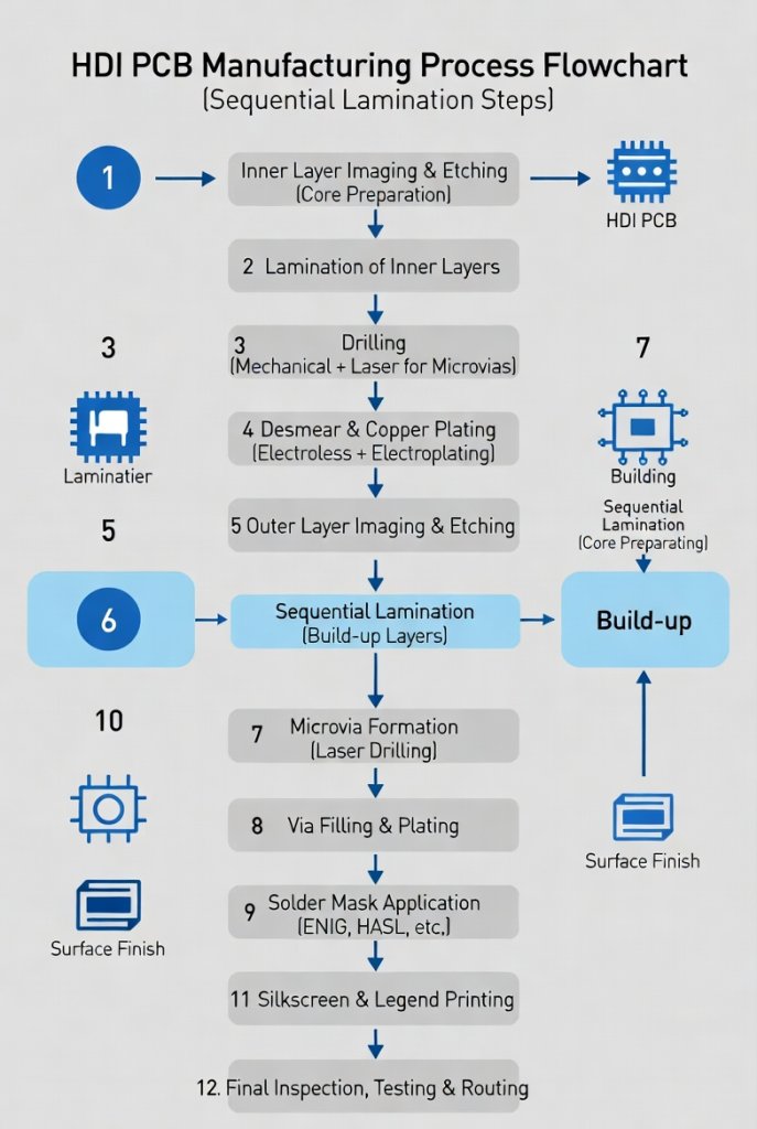
Step 6: Fine-Line Patterning and Final Processing
Laser Direct Imaging (LDI) technology achieves the precise alignment and resolution required for fine-line patterning. Final processing includes surface finish application (ENIG, OSP, or immersion tin), electrical testing, and quality inspection.
Quality Control Note: Factory analysis shows that X-ray inspection ensures copper fill void rates below 5%, and 100% flying probe testing verifies connectivity across all microvia interconnections — critical for ensuring long-term reliability in high-density boards.
HDI PCB Types and Stack-Up Structures
HDI PCBs are classified by the number of build-up layers and microvia configurations. Selecting the appropriate type depends on component density, BGA pitch, and signal integrity requirements.
Type 1 HDI (1-N-1)
- Structure: Single build-up layer on one or both sides of the core
- Vias: Blind microvias from outer layers to adjacent layers only
- Best for: Entry-level HDI designs, 0.5mm to 0.8mm pitch BGAs
- Manufacturing complexity: Lowest among HDI types
Type 2 HDI (2-N-2)
- Structure: Two build-up layers on each side, requiring two sequential lamination cycles
- Vias: Stacked or staggered blind/buried microvias
- Best for: Moderate-density designs, 0.4mm to 0.5mm pitch BGAs
- Example: A 6-layer 2-step HDI (2+2+2) with BGA 0.18mm pitch
Type 3 HDI (3+N+3 and Above)
- Structure: Three or more build-up layers, enabling complex routing scenarios
- Vias: Stacked microvias with any-layer interconnect capability
- Best for: High-density mobile devices, advanced automotive modules, AI servers
- Manufacturing complexity: Highest, requiring advanced fabrication equipment
Every Layer Interconnect (ELIC)
ELIC represents the most advanced HDI architecture, where microvias on every layer enable interconnection between any two layers in the stack-up. This technology is essential for cutting-edge smartphone motherboards and ultra-compact wearable devices.
| HDI Type | Build-Up Layers | Max BGA Pitch | Sequential Laminations | Typical Applications |
|---|---|---|---|---|
| Type 1 (1-N-1) | 1 per side | 0.5mm – 0.8mm | 1 | Industrial controls, basic consumer electronics |
| Type 2 (2-N-2) | 2 per side | 0.35mm – 0.5mm | 2 | Smartphones, tablets, automotive infotainment |
| Type 3 (3+N+3) | 3+ per side | 0.25mm – 0.4mm | 3+ | 5G devices, advanced ADAS, medical imaging |
| ELIC | All layers | < 0.35mm | 4+ | Flagship smartphones, premium wearables |
HDI PCB vs Traditional PCB: A Detailed Comparison
When evaluating whether HDI technology is appropriate for a specific project, engineers must understand the concrete differences between HDI and conventional PCB approaches.
| Feature | HDI PCB | Traditional PCB |
|---|---|---|
| Via Diameter | 0.10mm – 0.15mm (microvia) | 0.30mm – 0.50mm (mechanical drill) |
| Line/Space Width | ≤ 75µm (fine line) | ≥ 100µm (standard) |
| Layer Count (equivalent density) | 6 – 12 layers | 12 – 24+ layers |
| Min BGA Pitch Supported | 0.25mm – 0.40mm | ≥ 0.50mm |
| Signal Integrity at High Speed | Excellent (short via stubs) | Limited (long via stubs cause reflections) |
| Board Size (equivalent function) | 30% – 50% smaller | Larger footprint required |
| Weight | Significantly lighter | Heavier (more material) |
| Manufacturing Lead Time | 5 – 10 days (standard) | 3 – 7 days |
| Unit Cost (high volume) | Moderate premium | Lower base cost |
| Cost per Function/Area | Often lower overall | Higher when density is required |
Design Reality: While HDI PCB carries a moderate manufacturing premium, analysis shows that when evaluated on a cost-per-function basis, HDI often proves more economical — the reduction in layer count, board area, and component count typically offsets the higher processing costs, particularly in volumes above 1,000 units.
Industry Applications and Real-World Use Cases
HDI PCB technology serves diverse industries where miniaturization, performance, and reliability converge. Here are three detailed application scenarios that demonstrate HDI’s transformative impact.
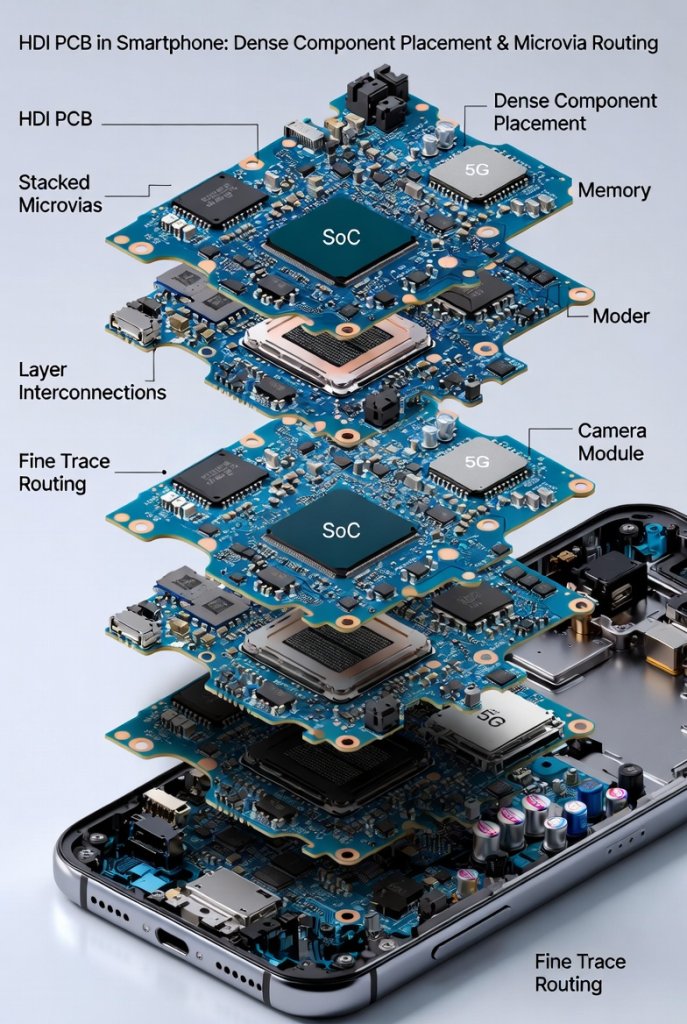
Use Case 1: 5G Smartphone Motherboard Manufacturing
The modern 5G smartphone represents one of the most demanding HDI applications. A flagship device motherboard typically employs 10+ layer HDI PCB with any-layer interconnect to accommodate:
- RF front-end complexity: Multiple frequency bands, MIMO antenna feeds, and millimeter-wave modules
- Application processor: High-pin-count SoC with 0.35mm pitch BGA requiring dense fanout
- Memory stacking: LPDDR5 packages alongside NAND flash in confined spaces
Industry Data: 5G smartphone motherboards require 10+ layer HDI PCBs to accommodate RF front-end module complexity within the constrained board dimensions imposed by battery capacity and camera module competition for internal device volume.
Smartphone OEMs rely on HDI PCB technology to achieve board areas below 3,000 mm² while supporting 5G data rates exceeding 10Gbps — impossible with conventional PCB approaches.
Use Case 2: Automotive ADAS Controller Modules
Advanced Driver Assistance Systems (ADAS) represent the fastest-growing segment for HDI PCB adoption, accounting for 33.9% of application share in 2026 according to market research.
A typical ADAS controller for Level 2+ autonomous driving requires:
- Multi-channel sensor fusion: Camera, radar, and LiDAR data processing in real-time
- High-reliability interconnects: Via structures tested to 15-year vehicle lifetime thermal cycling requirements
- Compact form factors: Integration into increasingly crowded vehicle electronics bays
Automotive Tier-1 suppliers pre-qualify HDI PCB vendors with IATF 16949 certification and automotive-grade microsection analysis capability to ensure via reliability across temperature ranges from -40°C to 150°C.
Use Case 3: Medical Portable Diagnostic Devices
Portable diagnostic devices illustrate HDI PCB’s contribution to healthcare technology. Modern handheld ultrasound devices, blood glucose monitors, and patient monitoring systems leverage HDI technology to achieve:
- Miniaturized form factors: Devices small enough for point-of-care and home healthcare settings
- High signal fidelity: Clean analog signal paths for accurate sensor readings
- Battery efficiency: Lower power consumption through optimized routing and reduced parasitic losses
The medical device segment projects a CAGR of approximately 8.1%, with portable diagnostic devices representing the largest subsegment driven by remote patient monitoring adoption.
Application Note: Wearable device miniaturization for smartwatches, wireless earbuds, and medical monitoring patches demands HDI PCBs with microvia stacking and any-layer interconnect capability to achieve functional circuit density within form factors below 100 mm² board area.
Use Case 4: Industrial IoT Edge Devices
Industrial Internet of Things (IIoT) edge computing modules represent an emerging high-growth application for HDI PCB technology. These devices must process sensor data locally while operating reliably in harsh factory environments:
- Multi-protocol wireless integration: Simultaneous Wi-Fi, Bluetooth, Zigbee, and LoRa connectivity in compact modules
- Real-time processing capability: ARM Cortex-class processors with external memory in space-constrained DIN-rail mountable enclosures
- Extended temperature operation: Reliable performance from -40°C to 85°C in industrial settings with minimal airflow
The industrial IoT segment’s growth directly correlates with Industry 4.0 adoption, where HDI PCB enables the compact form factors necessary for retrofitting smart connectivity into legacy manufacturing equipment without major redesigns of existing control panels.
HDI PCB Market Trends and Growth Data
Understanding market dynamics helps engineers and procurement teams anticipate supply chain developments and technology roadmaps.
Market Size and Projections
The global HDI PCB market demonstrates robust growth across all major research forecasts:
- 2025 market valuation: USD 19.50 – 19.61 billion
- 2033 – 2036 projection: USD 37.62 – 51.34 billion
- Compound Annual Growth Rate: 8.5% – 10.1% across forecast periods

Regional Manufacturing Landscape
| Region | 2026 Market Share | Growth Rate | Key Characteristics |
|---|---|---|---|
| Asia Pacific | 76.9% | 8.5%+ CAGR | China and Taiwan dominate production; largest manufacturing base |
| China specifically | — | 10.6% CAGR | Government policies strengthening domestic production; Zhen Ding, Fastprint lead |
| North America | ~25% | Steady | Strong in AI server and defense applications; 38% of AI Server HDI PCB market |
| Europe | 6.4% | Fastest growing | Automotive innovation hub (Germany); strict quality regulations driving precision demand |
Product Type Segmentation
Data from 2026 indicates that 4 to 6 layer HDI products command 44.7% of the product type market share, reflecting their versatility across the broadest application range. However, 10+ layer HDI represents the fastest-growing segment at approximately 11.8% CAGR, driven by 5G smartphone and AI server demands.
Key Technology Drivers
Several macro trends continue accelerating HDI PCB adoption:
- Automotive electronics proliferation: Per-vehicle semiconductor content exceeding USD 700 drives HDI adoption for ADAS, infotainment, and battery management
- 5G infrastructure deployment: Base station and handset requirements for high-frequency, high-density interconnects
- AI server expansion: GPU and accelerator cards requiring extremely dense routing for HBM memory interfaces
- Wearable device growth: Industry 4.0 and health monitoring trends creating demand for ultra-compact boards
- IoT module miniaturization: Connected sensors and edge devices requiring reliable operation in small form factors
Frequently Asked Questions (FAQ)
What is the difference between HDI PCB and standard PCB?
HDI PCB uses laser-drilled microvias (≤150µm), fine lines/spaces (≤75µm), and sequential lamination to achieve higher wiring density than standard PCBs. Standard PCBs rely on mechanically drilled through-holes (≥300µm) and wider trace widths. The result is that HDI PCBs can be 30% to 50% smaller while delivering superior signal integrity and supporting finer-pitch components like 0.35mm BGAs that standard PCBs cannot accommodate.
How much does HDI PCB manufacturing cost compared to conventional PCBs?
HDI PCB manufacturing typically carries a 20% to 50% premium over conventional PCBs at the bare board level, primarily due to sequential lamination cycles, laser drilling equipment, and specialized materials. However, when evaluated on a total system cost basis, HDI frequently proves more economical — the technology enables reduced layer counts (e.g., 8 layers vs. 16 layers), smaller board sizes, fewer components, and simplified assembly. For high-volume consumer electronics, the total cost savings often outweigh the HDI manufacturing premium.
What is the typical manufacturing lead time for HDI PCB prototypes?
Standard HDI PCB prototype lead times range from 5 to 10 business days depending on layer count and build-up complexity. A simple 1-step HDI (1-N-1) may deliver in 5 days, while a complex 3-step HDI with ELIC capability typically requires 10 to 15 days. Rush services from specialized manufacturers can reduce this to 72 hours for simpler HDI configurations. Lead times also vary by region — Asian manufacturers typically offer shorter turnaround than North American or European facilities.
Which industries use HDI PCB technology the most?
The top HDI PCB consuming industries by market share are:
- Automotive electronics (33.9%): ADAS controllers, infotainment systems, battery management modules
- Smartphones and mobile devices (30.3%): Motherboards, RF modules, camera subsystems
- Computing and AI servers: GPU accelerators, high-performance memory modules
- Medical devices: Portable diagnostics, implantable devices, surgical instruments
- Aerospace and defense: Ruggedized communication systems, avionics
What design considerations are critical for HDI PCB layout?
Successful HDI PCB design requires attention to several unique parameters beyond conventional board layout:
- Aspect ratio control: Maintaining 1:1 aspect ratio for microvias ensures reliable copper plating and minimizes void formation
- Material selection: Prepreg must be specifically formulated for laser drillability; standard FR-4 materials may not produce clean microvia walls
- Thermal management planning: Dense component placement requires careful via placement for heat dissipation, often using thermal microvia arrays beneath high-power components
- Fabricator engagement: Early collaboration with your HDI manufacturer ensures design for manufacturability (DFM) compliance and prevents costly revisions
- Stacked via registration: Multi-step HDI requires precise layer-to-layer alignment; designers should follow fabricator-specific tolerance guidelines
Engineering Best Practice: Contact your HDI fabrication partner before finalizing your PCB layout. Key information to obtain includes subtractive etching limits, laser drill depth and diameter capabilities, maximum stacked microvia limits, and via-in-pad finishing options. This proactive approach typically reduces design iterations by 30% to 40%.
What microvia structures are available in HDI PCB design?
HDI PCB supports three primary microvia configurations:
- Stacked microvias: Vertically aligned on consecutive layers, enabling the highest routing density but requiring precise registration and copper fill for reliability
- Staggered microvias: Offset placement across layers, offering improved thermal cycling reliability and simpler manufacturing at moderate density levels
- Via-in-pad: Microvias placed directly inside component pads, maximizing routing space beneath fine-pitch BGAs but requiring planarization for flat mounting surfaces
Conclusion: Is HDI PCB Right for Your Project?
HDI PCB technology has transitioned from a niche solution for premium devices to a mainstream manufacturing necessity across automotive, telecommunications, consumer electronics, and medical industries. As market data projects the industry expanding from USD 19.5 billion in 2025 to over USD 50 billion by 2036, the technology maturity and supply chain scale have reached points where HDI is accessible to a broader range of products than ever before.
Your project likely benefits from HDI PCB if it involves:
- BGA components with pitch below 0.5mm
- Strict size or weight constraints (portable/wearable devices)
- High-speed signals above 5Gbps requiring controlled impedance
- Layer count exceeding 12 in conventional PCB implementations
- Thermal or reliability requirements demanding optimized copper distribution
Final Recommendation: While HDI PCB involves higher upfront engineering and manufacturing costs, the analysis consistently shows that for density-critical applications, the total system cost — factoring in reduced board area, fewer layers, simplified assembly, and improved performance — often favors HDI over conventional approaches. Early engagement with an experienced HDI manufacturing partner during the design phase typically reduces iterations by 30% to 40% and prevents costly redesigns later in the development cycle.
Ready to explore HDI PCB for your next project? Contact Andwin Circuits — with long-standing HDI experience and 7+N+7 manufacturing capability — to discuss your requirements and receive a detailed quote for your high-density interconnect PCB needs.