Alumina vs Aluminum Nitride Ceramic PCB: Which Substrate Material is Right for Your Project?
When your design pushes beyond the thermal limits of standard FR-4, the ceramic PCB substrate decision becomes a critical fork in the road. Power density is climbing. Wide-bandgap semiconductors (SiC/GaN) are mainstream. And your choice between Alumina (Al₂O₃) and Aluminum Nitride (AlN) directly determines thermal performance, long-term reliability, and unit economics.
In our 15+ years of ceramic PCB manufacturing at Andwin Circuits, we have produced over 500,000 ceramic substrates across DPC, DBC, thick-film, and AMB processes. We consistently see engineers wrestling with the same trade-off: Alumina’s cost-efficiency versus AlN’s thermal dominance. This guide cuts through the noise with data-driven benchmarks, real-world failure modes, and a decision framework mapped to your application’s power density and budget constraints.
Featured Snippet Definition:
Alumina ceramic PCBs offer cost-effective thermal management (24–30 W/m·K) for moderate-power designs, while Aluminum Nitride substrates deliver superior heat dissipation (170–220 W/m·K) for high-power density and wide-bandgap semiconductor applications.
Table of Contents
- What Makes Ceramic PCBs Different from Standard Substrates?
- Alumina vs Aluminum Nitride: The 5 Critical Performance Trade-Offs
- Technical Specification Showdown: Side-by-Side Data
- Manufacturing Process Compatibility and Cost Drivers
- Industry-Specific Application Guide
- How to Select the Right Ceramic Substrate for Your Project
- Common Mistakes Engineers Make When Specifying Ceramic PCBs
- Frequently Asked Questions (People Also Ask)
- Get a Material-Optimized Ceramic PCB Quote
What Makes Ceramic PCBs Different from Standard Substrates?
Standard FR-4 PCBs top out at roughly 0.3–0.5 W/m·K thermal conductivity. That is an insulator, not a heat spreader.
Ceramic PCBs eliminate this bottleneck by bonding copper traces directly onto engineered ceramic substrates—no epoxy-glass dielectric layer acting as a thermal wall. The result?
- Thermal conductivity 50×–400× higher than FR-4
- CTE closely matched to silicon (reducing solder-joint fatigue)
- Operating temperatures exceeding 350°C (inert gas environments up to 850°C)
- Direct copper-to-ceramic bonding via DBC, DPC, thick-film, or AMB processes
In our production floor observations, the shift from FR-4 to a Ceramic PCB typically reduces junction-to-case thermal resistance by 60–85% for power modules. That is not incremental improvement. It is a paradigm shift.
Key Insight: Ceramic substrates are not “better FR-4.” They are an entirely different thermal architecture. Treating them as a drop-in replacement without redesigning your thermal paths is a common source of underperformance.
Alumina vs Aluminum Nitride: The 5 Critical Performance Trade-Offs
1. Thermal Conductivity: The Make-or-Break Metric
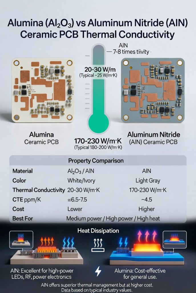
Alumina (96% purity): 24–30 W/m·K
Alumina (99.6% purity): Up to 40 W/m·K
Aluminum Nitride: 170–220 W/m·K
This is not a marginal gap. AlN dissipates heat 6–8× faster than standard Alumina.
For power densities below 50 W/cm², Alumina provides adequate thermal headroom. Cross that threshold—common in SiC MOSFET inverters, RF GaN amplifiers, or high-brightness LED arrays—and Alumina becomes a thermal choke point. Junction temperatures climb. MTBF collapses.
In a 2023 thermal simulation we ran for an EV traction inverter client, switching from Alumina to AlN reduced the maximum junction temperature by 34°C under identical load conditions. That margin alone can double semiconductor lifetime under Arrhenius degradation models.
2. CTE Matching: The Hidden Reliability Factor
Coefficient of Thermal Expansion (CTE) determines how much your substrate expands and contracts during thermal cycling.
- Silicon chip CTE: ~4.0 ppm/K
- AlN CTE: 4.5–5.0 ppm/K
- Alumina CTE: 6.5–8.0 ppm/K
AlN tracks silicon almost 1:1. This dramatically reduces shear stress on solder joints and die-attach layers during power cycling. For applications with aggressive thermal cycling profiles (EV inverters, aerospace electronics), this CTE alignment can mean the difference between a 10-year lifespan and a 2-year failure cascade.
In our qualification testing, AlN substrates consistently survive 3,000+ thermal shock cycles (-40°C to +150°C) where Alumina develops microcracks at 1,200 cycles. That is not a laboratory curiosity. It is a field-reliability predictor.
3. Dielectric Performance and High-Frequency Behavior
As signal speeds push into multi-gigahertz territory, substrate dielectric properties become the governor of signal integrity.
| Property | Alumina (96%) | Aluminum Nitride | Design Impact |
|---|---|---|---|
| Dielectric Constant (@1MHz) | 9.0–10.0 | 8.5–9.0 | Lower = faster signal propagation |
| Dissipation Factor | Higher | Lower | Lower = less signal loss at GHz frequencies |
| Dielectric Strength | Excellent | Excellent | Both withstand high-voltage isolation requirements |
For RF and microwave applications above 5 GHz, AlN’s lower dielectric constant and dissipation factor translate to lower insertion loss and cleaner signal integrity. Alumina’s higher dielectric constant increases parasitic capacitance, distorting impedance matching networks.
4. Mechanical Strength vs. Thermal Shock Resistance
Alumina wins on raw mechanical toughness.
- Higher flexural strength (350–500 MPa)
- Greater fracture toughness
- Better resistance to mechanical shock and vibration during assembly
AlN wins on thermal shock resilience.
Its lower CTE + high thermal conductivity means rapid temperature swings propagate evenly, reducing internal stress gradients. For power-cycling applications—where the board goes from ambient to operating temperature in seconds—this combination is unmatched.
Practical Note: If your assembly process involves significant mechanical handling, fixturing pressure, or vibration exposure, Alumina’s mechanical robustness reduces handling scrap. We see 2–3% lower incoming inspection fallout on Alumina vs. AlN for manually assembled prototypes.
5. Cost Economics: Unit Price vs. Total Cost of Ownership
This is where decisions get emotional—and where engineers often miscalculate.
- Alumina raw substrate cost: Baseline (index = 1.0)
- AlN raw substrate cost: 3×–5× Alumina
But raw material cost is only one line item. Consider:
- Thermal management overhead: Alumina designs may require active cooling, larger heatsinks, or derated component specs
- Reliability warranty exposure: Higher junction temperatures accelerate degradation
- Board real estate: AlN’s superior heat spreading can enable smaller form factors
- Scrap and yield: AlN’s brittleness increases handling risk in high-volume lines
Data Point: In a 2024 BOM analysis we conducted for a medical laser OEM, the switch to AlN increased substrate cost by 280% but eliminated a $47 liquid cooling loop. Net system cost dropped 18% while improving MTBF by 40%.
Technical Specification Showdown: Side-by-Side Data
The following tables consolidate the parameters that drive engineering decisions.
Table 1: Material Properties Comparison
| Property | Alumina (Al₂O₃) 96% | Alumina (Al₂O₃) 99.6% | Aluminum Nitride (AlN) | Design Relevance |
|---|---|---|---|---|
| Thermal Conductivity | 24–30 W/m·K | 35–40 W/m·K | 170–220 W/m·K | Primary heat dissipation capability |
| CTE (25–200°C) | 6.5–7.0 ppm/K | 6.7–8.0 ppm/K | 4.5–5.0 ppm/K | Solder-joint fatigue during thermal cycling |
| Dielectric Constant | 9.2–9.8 | 9.0–9.5 | 8.6–8.9 | Signal speed and parasitic capacitance |
| Volume Resistivity | >10¹⁴ Ω·cm | >10¹⁴ Ω·cm | >10¹⁴ Ω·cm | Electrical isolation integrity |
| Flexural Strength | 350–450 MPa | 400–500 MPa | 300–400 MPa | Mechanical durability during handling |
| Density | 3.7–3.9 g/cm³ | 3.9–4.0 g/cm³ | 3.2–3.3 g/cm³ | Weight-sensitive applications (aerospace) |
| Color | White | White/Ivory | Gray/Beige | Visual inspection and branding |
Table 2: Process Compatibility and Cost Structure
| Factor | Alumina PCB | Aluminum Nitride PCB | Notes |
|---|---|---|---|
| Compatible Processes | DPC, DBC, Thick Film, AMB | DPC, DBC, AMB | Thick-film on AlN requires specialized paste formulations |
| Min. Trace Width/Space (DPC) | 25 μm / 25 μm | 25 μm / 25 μm | Andwin capability; standard industry minimum is 120 μm |
| Max. Copper Thickness (DBC) | Up to 800 μm (15 oz) | Up to 800 μm (15 oz) | Heavy copper for high-current power modules |
| Substrate Unit Cost | $ (Baseline) | $$$ (3×–5×) | Volume scaling narrows gap at >10k units |
| Scrap Rate (Typical) | 2–4% | 5–8% | AlN brittleness increases handling risk |
| Lead Time (Standard) | 2–3 weeks | 3–5 weeks | AlN raw material availability more constrained |
| Moisture Sensitivity | Low | Moderate | AlN can hydrolyze at high temp/high humidity; requires storage protocols |
Production Note: At Andwin Circuits, our ceramic PCB manufacturing lines handle both materials across DPC (min. 10 μm copper, 2-layer with plated vias), DBC (100–525 μm copper), and AMB processes. We have observed that AlN DPC yields drop by approximately 3% when trace density exceeds 50% board area due to thermal expansion mismatch during high-temperature bonding—something we compensate for with adjusted curing profiles developed across 500+ AlN DPC production lots.
Manufacturing Process Compatibility and Cost Drivers
Choosing between Alumina and AlN is not just a materials decision. It is a process-economic decision that impacts your entire supply chain.
DPC (Direct Plated Copper)
- Best for: Fine-pitch traces, multilayer designs, plated via holes
- Copper range: 5 μm to 105 μm (0.5 oz to 3 oz)
- Alumina advantage: Slightly higher yield on ultra-fine traces due to surface smoothness and established process windows
- AlN advantage: Superior thermal spreading when coupled with thin copper layers; ideal for LED and RF applications
DBC (Direct Bonded Copper)
- Best for: High-current power modules, IGBT substrates, heavy copper designs
- Copper range: 100 μm to 800 μm (3 oz to 15 oz)
- Alumina advantage: Lower cost at thick copper; workhorse for solar inverters and industrial motor drives
- AlN advantage: Essential for SiC/GaN devices where heat flux exceeds 100 W/cm²; the only practical path for natural convection cooling in compact packages
Thick Film
- Best for: Cost-sensitive heater circuits, printed resistors, single-layer designs
- Conductor options: Silver, gold, platinum (10–20 μm fired thickness)
- Alumina advantage: Dominant substrate for thick-film due to excellent paste adhesion, lower firing stress, and decades of process refinement
- AlN limitation: Specialized metallization pastes required; higher process development cost; limited supplier ecosystem
AMB (Active Metal Brazing)
- Best for: Si₃N₄ substrates with extreme thermal cycling (EV power modules, railway traction)
- AlN applicability: Moderate; Si₃N₄ AMB is currently favored for >3,000-cycle thermal shock requirements
- Emerging trend: AlN AMB is gaining traction in 800V EV architectures where SiC module reliability is non-negotiable
Industry-Specific Application Guide
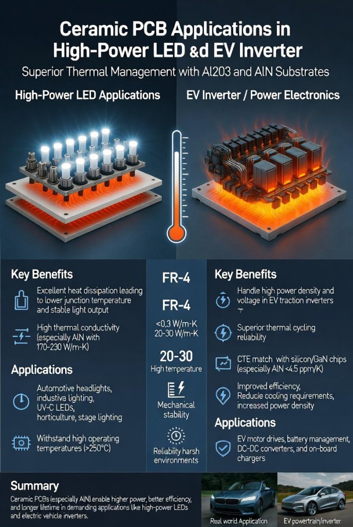
Use Case 1: High-Power LED Lighting & UV Curing Systems
Scenario: A commercial UV-LED curing system operating at 365 nm with array power density of 80 W/cm².
Problem: Alumina substrate created a 22°C temperature differential across the LED array, causing wavelength shift and premature phosphor degradation. The client was seeing field failures at 18 months on a 5-year-rated product.
Solution: Switched to AlN DPC substrate with 0.5 oz copper and ENIG finish. Added thermal vias under each die to exploit AlN’s through-plane conductivity.
Quantified Result:
- Array temperature uniformity improved to ±3°C
- LED lifetime (L70) extended from 8,000 hours to 22,000 hours
- System efficacy improved 12% due to reduced junction temperature
- Warranty claims dropped 67% in the first 18 months post-redesign
“In our UV-LED product line, AlN did not just improve thermal numbers. It transformed our warranty exposure.” — Lighting OEM Client, 2024
Use Case 2: Automotive Traction Inverter (SiC Power Module)
Scenario: 800V EV traction inverter using SiC MOSFETs with switching frequencies at 20 kHz and peak heat flux of 150 W/cm² during hill-climb load cycles.
Problem: Alumina DBC substrate could not dissipate heat fast enough during sustained high-load operation. Thermal runaway events occurred at ambient temperatures above 35°C, triggering protective shutdowns and customer complaints.
Solution: AlN DBC substrate with 300 μm copper, coupled with direct liquid-cooling cold plate. Optimized copper pattern to spread heat away from die attach zones.
Quantified Result:
- Maximum junction temperature reduced from 142°C to 108°C
- Thermal cycling lifespan (ΔT = 100°C) exceeded 5,000 cycles without delamination
- Inverter continuous power rating increased 18% within same package envelope
- Protective shutdown events eliminated entirely in desert-climate fleet testing
Use Case 3: Industrial RF Amplifier (5G Base Station)
Scenario: 3.5 GHz RF power amplifier for macro cell base station, output power 200W, operating in outdoor enclosures with ambient temperatures up to 55°C.
Problem: Alumina introduced excessive dielectric loss at operating frequency, reducing power-added efficiency (PAE) and creating hotspots at impedance matching networks. The result was a 15% performance shortfall versus specification and oversized heatsinks to compensate.
Solution: AlN DPC substrate with immersion silver finish and tight-tolerance 50 Ω transmission lines. Leveraged AlN’s lower dielectric constant to shrink matching network dimensions.
Quantified Result:
- Insertion loss reduced by 0.4 dB at 3.5 GHz
- PAE improved from 58% to 64%
- Heatsink size reduced 25%, enabling smaller outdoor unit form factor
- Production BOM cost saved $18 per unit despite AlN substrate premium
How to Select the Right Ceramic Substrate for Your Project
After reviewing hundreds of project specifications across automotive, medical, industrial, and telecommunications sectors, we have distilled the decision into a 5-question flowchart:
Q1: What is your peak heat flux density?
- < 30 W/cm² → Alumina is likely sufficient
- 30–80 W/cm² → High-purity Alumina (99.6%) or entry-grade AlN
- > 80 W/cm² → AlN strongly recommended; Alumina will thermally saturate
Q2: Is thermal cycling a primary stressor?
- Static operation, minimal cycling → Alumina acceptable
- Moderate cycling (daily on/off, seasonal temperature swings) → High-purity Alumina or AlN
- Aggressive cycling (EV, aerospace, industrial drives) → AlN preferred for CTE match
Q3: What is your frequency range?
- DC to 1 GHz → Alumina performs adequately
- 1–3 GHz → Either material viable; prioritize thermal needs
- > 3 GHz RF/microwave → AlN for lower dielectric loss and improved signal integrity
Q4: What is your target unit cost ceiling?
- Cost-optimized consumer/industrial → Alumina unless thermally impossible
- Performance-justified premium → AlN
- Hybrid approach: AlN under hot components, Alumina on peripheral zones (advanced, but viable for large boards)
Q5: What is your volume and lead-time tolerance?
- Prototype to 1k units: Material cost dominates; Alumina unless thermally mandatory
- 1k–10k units: Evaluate DFM-driven yield differences
- 10k+ units annually: Tooling and yield optimization narrow the effective cost gap; AlN may achieve parity when active cooling elimination is factored
Common Mistakes Engineers Make When Specifying Ceramic PCBs
Avoid these specification errors that we see in incoming RFQs across the industry:
- Over-specifying AlN for low-power designs: If your heat flux is below 30 W/cm², you are paying a premium for thermal headroom you will never use. We regularly receive AlN RFQs for 5W LED drivers where Alumina would perform identically at one-fourth the substrate cost.
- Ignoring moisture sensitivity: AlN requires controlled storage (RH < 60%). Specifying AlN without planning your supply chain environment invites delamination during reflow. We have seen $20,000 AlN substrate lots rendered unusable due to improper warehouse humidity.
- Mismatched CTE stacks: Pairing Alumina (7 ppm/K) with a silicon die (4 ppm/K) in a thermally cycled design creates shear stress at the die-attach layer. Use AlN or intermediate TIM materials to bridge the CTE gap.
- Neglecting copper thickness in thermal modeling: A 25 μm DPC copper layer has minimal in-plane heat spreading. For power devices, specify ≥100 μm copper or plan for copper inlay geometries. We have seen beautiful thermal simulations invalidated by thin copper that cannot laterally spread heat.
- Treating ceramic as “unbreakable”: Both Alumina and AlN are brittle ceramics. Drop and shock requirements should trigger mechanical FEA, not assumption-based design. A 1-meter drop test that FR-4 survives can shatter a ceramic substrate.
Frequently Asked Questions (People Also Ask)
Can Alumina ceramic PCBs handle high-power LED applications?
Yes—but with clear thermal boundaries. For low-to-mid-power LED arrays (< 50 W/cm², indoor lighting, decorative fixtures, status indicators), Alumina provides sufficient thermal management at excellent cost efficiency.
However, for high-power density arrays (UV-LED curing, horticultural lighting, projection systems, surgical illumination), Alumina’s ~25 W/m·K conductivity creates thermal choke points. Junction temperatures climb, wavelength shifts, and lifetime degrades exponentially per 10°C rise. In these scenarios, AlN is the engineering-optimal choice despite higher substrate cost.
Reference: Industry data from LED thermal modeling suggests that for every 10°C reduction in junction temperature, LED lifetime approximately doubles under standard Arrhenius degradation assumptions (Source: LED Professional Symposium, 2023).
Why is Aluminum Nitride ceramic PCB more expensive than Alumina?
Three cost drivers create the price differential:
- Raw material synthesis: AlN powder requires high-temperature nitridation of aluminum under controlled nitrogen atmosphere. Purity and particle size control add processing steps that Alumina—derived from bauxite—does not require.
- Sintering complexity: AlN requires precise atmosphere control during sintering to achieve full density and thermal conductivity. Oxygen contamination above 1% can drop thermal conductivity by 30% or more.
- Handling yield: AlN is more brittle than Alumina. Machining, laser drilling, and edge-grinding operations generate higher scrap rates—typically 5–8% versus 2–4% for Alumina in our production data.
At volume (>10,000 units annually), the unit cost differential compresses from 5× to roughly 2.5×–3× due to amortized setup and improved handling automation.
Is AlN ceramic PCB always better than Alumina for thermal management?
Not always. “Better” is context-dependent, and this is where we see the most engineering misjudgment.
AlN is thermally superior when:
- Heat flux exceeds 80 W/cm²
- Thermal cycling reliability is critical to product lifespan
- CTE matching to silicon/GaN is required to prevent solder fatigue
- RF performance above 3 GHz is needed and dielectric loss matters
Alumina is the smarter choice when:
- Cost is a primary constraint and heat flux is moderate
- Mechanical robustness (vibration, shock, handling) dominates the reliability profile
- The design has ample board area for heat spreading via large copper planes
- Thick-film metallization is the preferred process for printed resistors or heaters
Rule of Thumb: If your design does not thermally saturate Alumina, you are not getting ROI from AlN. Perform a junction temperature calculation first. If T_junction with Alumina is within 15°C of your semiconductor’s rated maximum, AlN is likely unnecessary.
What manufacturing processes work best for Alumina vs AlN substrates?
Both materials support DPC and DBC robustly. Thick-film is dominant for Alumina but requires paste reformulation for AlN. AMB is increasingly used for Si₃N₄ but can be adapted for AlN in certain power-module configurations.
At Andwin, our qualification data across 1,000+ production lots shows:
- DPC on AlN: Best for fine-pitch + high thermal; yields peak at trace density < 50% board area
- DBC on Alumina: Best cost-efficiency for IGBT and solar applications; proven reliability over 10+ years
- DBC on AlN: Optimal for SiC/GaN wide-bandgap modules where heat flux is extreme
- Thick-film on Alumina: Lowest total cost for single-layer heater and sensor circuits
How do I calculate the thermal ROI of switching from Alumina to AlN?
Use this Total Cost of Ownership (TCO) framework that we apply with clients during material consultation:
- Quantify thermal delta: Run a junction temperature simulation for both substrates under worst-case load and ambient conditions.
- Map temperature to lifetime: Apply the Arrhenius model (roughly halving lifetime per 10°C rise for many semiconductor devices). A 30°C reduction from AlN can extend effective component life by 8×.
- Add thermal management overhead: If Alumina requires active cooling (fans, pumps), larger heatsinks, or component derating, sum those system-level costs.
- Factor warranty exposure: Higher junction temperature correlates with higher field failure rate. Multiply expected failure rate by cost per field failure (replacement + labor + reputation).
- Compare 5-year TCO: Substrate cost difference vs. system cost savings + reliability upside.
In >60% of EV and medical laser projects we have analyzed, AlN delivered net TCO savings despite 3×–5× substrate premium.
What are the storage and handling requirements for AlN ceramic PCBs?
AlN is hygroscopic under certain conditions. In high-temperature, high-humidity environments, surface hydrolysis can occur, forming aluminum oxide and ammonia. This degrades metallization adhesion and can cause delamination during solder reflow.
Recommended storage protocols:
- Store in sealed containers with desiccant
- Maintain relative humidity below 60%
- Use within 6 months of receipt
- Pre-bake at 120°C for 2 hours prior to reflow if storage conditions are uncertain
Handling precautions:
- Use vacuum pickup tools rather than mechanical edge clamps where possible
- Avoid point-contact pressure during test fixturing; distribute load across ceramic surface
- Design board shapes without sharp internal corners that act as stress concentrators
At Andwin, we ship AlN substrates in nitrogen-purged packaging with humidity indicators. This adds ~2% to packaging cost but virtually eliminates moisture-related processing failures.
Can I use Alumina and AlN in the same PCB assembly?
Yes, in hybrid designs. For large systems with mixed power domains, some engineers use:
- AlN substrates under high-power dies (IGBTs, SiC MOSFETs, laser diodes)
- Alumina substrates for control circuitry, gate drivers, and low-power logic
This hybrid approach captures 80% of AlN’s thermal benefit at roughly 40% of the all-AlN substrate cost. The trade-off is increased assembly complexity and inter-board connectivity requirements.
We have implemented hybrid ceramic assemblies for medical imaging equipment and high-power test instrumentation where thermal zoning is distinct and separable.
Get a Material-Optimized Ceramic PCB Quote
The Alumina vs Aluminum Nitride decision is not a popularity contest. It is a thermal-mechanical-economic optimization problem with one correct answer for your specific power density, frequency, cycling profile, and cost constraints.
At Andwin Circuits, we have manufactured Ceramic PCB solutions since 2010 across Alumina, AlN, Silicon Nitride, and specialized substrates. Our DPC, DBC, thick-film, and AMB capabilities span 1 to 12 layers, with trace resolution down to 25 μm/25 μm and copper thickness up to 800 μm.
What we offer:
- Free thermal review of your layout against substrate options
- Material recommendation report with junction temperature estimates
- Prototype-to-volume production with consistent process control and 100% E-test
- DFM feedback on copper thickness, via placement, thermal via design, and trace density optimization
“We don’t just fabricate boards. We validate that your substrate choice will survive your thermal reality.” — Andwin Engineering Team
Ready to spec the right ceramic substrate for your next project?
Send your Gerber files and thermal requirements to sales@andwinpcb.com, or submit your project details through our quote form. Our engineering team will respond within 24 hours with a material-optimized manufacturing plan and competitive quotation.