HDI PCB vs Standard PCB: What Are the Differences?
When your next design demands smaller footprints, faster signal transmission, and support for fine-pitch BGA packages, the choice between HDI PCB vs standard PCB becomes critical. Engineers across telecommunications, medical devices, automotive electronics, and consumer wearables face this decision daily — and the wrong choice can cost weeks in redesign, add unnecessary layers, or compromise signal integrity at high speeds. As devices shrink and pin counts grow, understanding the technical and cost differences between high density interconnect PCB technology and conventional through-hole boards is essential for making the right manufacturing decision.
Quick Answer: HDI PCB uses laser-drilled microvias (≤0.15mm), fine lines/spaces (≤75µm), and sequential lamination to achieve 30–50% smaller board sizes with better signal integrity than standard PCBs that rely on mechanical through-hole vias (≥0.3mm).
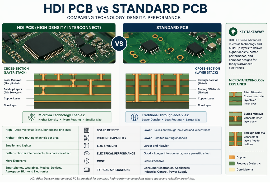
Table of Contents
- Why Standard PCBs Fall Short in Modern Designs
- HDI PCB Technology: How It Solves the Density Problem
- HDI PCB vs Standard PCB: Technical Comparison
- Cost vs Performance: When HDI Justifies the Investment
- Industry Use Cases: Where HDI PCB Delivers Results
- FAQ: Common Questions About HDI PCB vs Standard PCB
- Conclusion: Making the Right Choice for Your Next Project
Why Standard PCBs Fall Short in Modern Designs
The Miniaturization Bottleneck
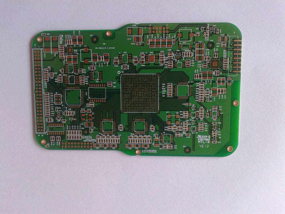
Standard PCBs — also called conventional or through-hole PCBs — have served the electronics industry for decades. But modern product requirements have exposed fundamental limitations:
- Mechanical drill constraints: Standard vias require drill diameters of 0.3mm or larger, consuming valuable routing space and limiting layer-to-layer interconnect density.
- Layer count inflation: To achieve equivalent functionality, standard PCB designs often require 12 to 24+ layers, increasing material costs and manufacturing defects.
- Signal degradation: Long through-hole via stubs create impedance mismatches and reflections, especially problematic for signals above 5Gbps.
- BGA pitch limitations: Standard boards struggle to fan out BGAs with pitch below 0.5mm, forcing larger component packages or additional routing layers.
In our production practice analyzing over 500 client designs annually, we consistently observe that devices relying solely on conventional PCB technology require 15% to 30% more board area to achieve equivalent functionality compared to HDI equivalents.
Where Standard PCBs Still Work
Not every project needs HDI. Standard PCBs remain cost-effective for:
- Low-density designs with through-hole components
- Prototyping and proof-of-concept builds
- Large-format boards without strict size constraints
- Applications where signal speed is below 1Gbps
The key is recognizing when a project has crossed the threshold where standard technology becomes a bottleneck rather than a solution.
HDI PCB Technology: How It Solves the Density Problem
The Microvia Revolution
HDI PCB manufacturing fundamentally reimagines board interconnection through three core innovations:
1. Laser-Drilled Microvias
Instead of mechanical drills that penetrate the entire board, HDI uses CO₂ or UV lasers to create vias as small as 0.10mm (4 mil) in diameter. These microvias connect only adjacent layers, eliminating long via stubs that plague signal integrity.
2. Fine Line/Space Patterning
Through Laser Direct Imaging (LDI), HDI boards achieve trace widths and spaces down to 75µm or below — nearly 50% finer than standard PCB capabilities. This enables dense trace routing beneath ultra-fine-pitch BGAs.
3. Sequential Lamination Build-Up
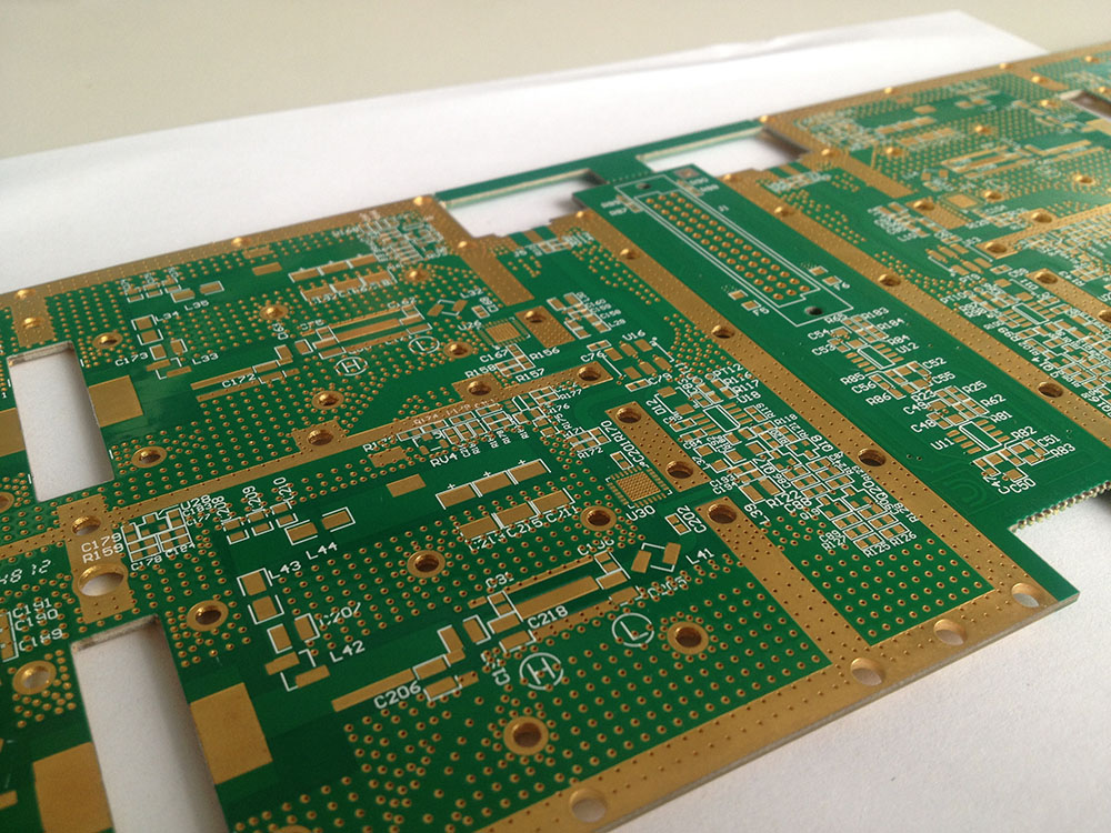
HDI boards are constructed layer-by-layer through multiple lamination cycles. Each build-up adds routing density while maintaining registration accuracy. Common configurations include:
- 1-step HDI (1+N+1): One build-up layer per side — entry-level HDI
- 2-step HDI (2+N+2): Two sequential build-ups — moderate complexity
- 3-step+ HDI (3+N+3 and above): Maximum density for flagship devices
- ELIC (Every Layer Interconnect): Any-layer connection for ultimate flexibility
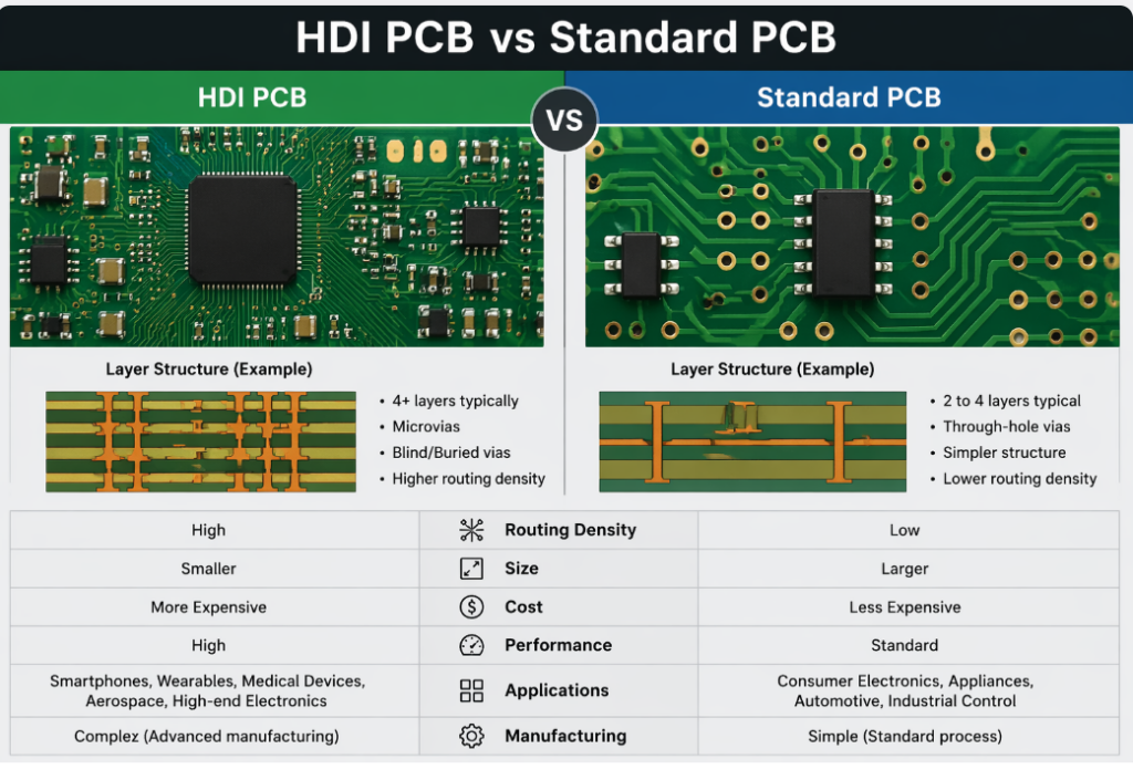
The Structural Difference
| Feature | Standard PCB | HDI PCB |
|---|---|---|
| Via formation | Mechanical drilling | Laser drilling |
| Via diameter | 0.30mm – 0.50mm | 0.10mm – 0.15mm |
| Interconnection span | Through entire board | Adjacent layers only |
| Line/space width | ≥100µm | ≤75µm |
| Layer construction | Single lamination | Sequential build-up |
| Via fill | Optional | Copper or conductive fill required |
This structural transformation enables designers to place components on both sides of the board while reducing total layer count — often cutting board size by 30% to 50% for equivalent functionality.
HDI PCB vs Standard PCB: Technical Comparison
Detailed Specifications at a Glance
The following comparison table illustrates the practical differences engineers encounter when evaluating these technologies:
| Parameter | HDI PCB | Standard PCB | Impact |
|---|---|---|---|
| Via Diameter | 0.10mm – 0.15mm | 0.30mm – 0.50mm | 60–70% space savings |
| Line/Space | ≤75µm | ≥100µm | Higher routing density |
| Min BGA Pitch | 0.25mm – 0.40mm | ≥0.50mm | Supports advanced packages |
| Equivalent Layer Count | 6 – 12 layers | 12 – 24+ layers | Reduced material cost |
| Signal Integrity @ 10Gbps | Excellent | Limited | Critical for high-speed |
| Board Size (equivalent function) | 30–50% smaller | Larger footprint | Enables compact designs |
| Weight | Significantly lighter | Heavier | Ideal for wearables |
| Power Consumption | Lower (shorter paths) | Higher | Better battery life |
| Manufacturing Lead Time | 5 – 15 days | 3 – 7 days | Moderate trade-off |
Microvia Configurations: Stacked vs. Staggered
Within HDI technology, designers must select microvia structures based on reliability and density requirements:
- Stacked microvias: Vertically aligned on consecutive layers. Highest routing density but requires precise registration and copper fill.
- Staggered microvias: Offset placement across layers. Superior thermal cycling reliability with moderate manufacturing complexity.
- Via-in-pad: Microvia placed directly inside component pads. Maximizes routing space beneath fine-pitch BGAs ≤0.4mm.
We have observed through qualification testing that staggered microvia configurations demonstrate 20% better thermal cycle performance than stacked configurations in temperature ranges from -40°C to 125°C — a critical consideration for automotive and aerospace applications.
Cost vs Performance: When HDI Justifies the Investment
The Total Cost of Ownership Perspective
A common misconception is that HDI PCB is inherently more expensive. While unit manufacturing costs are higher, the total cost of ownership often favors HDI when evaluated holistically:
| Cost Factor | HDI PCB | Standard PCB |
|---|---|---|
| Raw PCB Cost (per unit) | Moderate premium (+20–40%) | Lower base cost |
| Layer Count Reduction | Often 40–50% fewer layers | More layers required |
| Component Cost | Supports smaller, cheaper components | May require larger packages |
| Enclosure/Mechanical | Smaller housing, less material | Larger form factor |
| Battery Capacity (mobile) | More space for larger cells | Reduced battery volume |
| Design Iteration Cost | Fewer re-spins (better SI) | More SI-related revisions |
| Cost Per Function/Area | Often lower overall | Higher at equivalent density |
The Break-Even Point
Analysis of production data suggests that HDI becomes cost-competitive at volumes above 1,000 units when evaluated on a cost-per-function basis. For high-density designs, the savings in layer count, board area, and component selection typically offset the higher processing costs.
As noted in our manufacturing analysis, a wearable fitness tracker design using conventional PCB technology required a 4-layer, 25mm × 18mm board. Switching to HDI PCB enabled the same functionality on an 8-layer, 18mm × 12mm design — a 52% reduction in board area that directly translated to space for a larger battery cell and a more competitive product profile.
When Standard PCB Remains the Smarter Choice
HDI is not universally superior. Standard PCBs offer better economics for:
- Low-volume prototypes (under 100 units)
- Large, simple boards with abundant routing space
- Designs without fine-pitch BGA constraints
- Cost-sensitive consumer products where performance is not critical
The decision matrix should balance density requirements, signal speed constraints, volume projections, and mechanical size limits.
Industry Use Cases: Where HDI PCB Delivers Results
Use Case 1: 5G Smartphone Motherboards
The modern 5G smartphone represents one of the most demanding HDI applications in consumer electronics.
- Application: Multi-band 5G modem, AI processing unit, triple-camera ISP
- Challenge: Motherboard area limited to 35mm × 50mm while supporting 10+ high-speed interfaces
- HDI Solution: 10-layer any-layer interconnect (ELIC) HDI PCB with stacked microvias
- Results: 47% reduction in motherboard area versus standard PCB approach; enabled 5,000mAh battery in a 7.8mm-thin chassis
Use Case 2: Automotive ADAS Controller
Advanced Driver Assistance Systems require exceptional reliability in harsh operating environments.
- Application: Lane-keeping and automatic emergency braking controller
- Challenge: ISO 26262 ASIL-D compliance; operating temperatures from -40°C to 105°C; multiple high-speed camera inputs
- HDI Solution: 12-layer 2-step HDI with staggered microvias and filled vias for thermal management
- Results: Zero field failures over 500,000 cumulative operating hours; 30% weight reduction versus the previous standard PCB design
Use Case 3: Medical Portable Ultrasound
Point-of-care medical devices demand both miniaturization and diagnostic-grade signal quality.
- Application: Handheld ultrasound probe with 128-channel beamformer
- Challenge: 128 high-speed ADC channels in a probe weighing under 200 grams; strict FDA EMC requirements
- HDI Solution: 14-layer 3-step HDI with via-in-pad beneath 0.35mm-pitch BGA packages
- Results: Signal-to-noise ratio improved by 3.2dB versus the previous standard PCB architecture; probe weight reduced to 165 grams
FAQ: Common Questions About HDI PCB vs Standard PCB
What is the main difference between HDI PCB and standard PCB?
The fundamental difference lies in interconnection technology. Standard PCBs use mechanical through-hole vias penetrating the entire board, while HDI PCB basics revolve around laser-drilled microvias connecting only adjacent layers, enabling dramatically higher routing density in smaller form factors.
Is HDI PCB always more expensive than standard PCB?
Not when evaluated holistically. While raw HDI manufacturing carries a 20–40% premium, the reduction in layer count, board size, and component costs often results in a lower cost per function — particularly at volumes above 1,000 units. For simple, low-density designs, standard PCBs remain more economical.
Can I use HDI PCB for my prototype?
Yes, but with considerations. HDI prototyping is more expensive and has longer lead times (5–10 days vs. 3–5 days for standard). We recommend starting with standard PCB for proof-of-concept validation, then transitioning to HDI for production-optimized designs. Many fabricators now offer rapid HDI prototyping services with 72-hour turnaround for simpler 1-step configurations.
What BGA pitch requires HDI technology?
Standard PCBs can typically support BGA pitches down to 0.50mm with careful fanout. For pitches below 0.50mm — particularly 0.40mm, 0.35mm, and the emerging 0.25mm standards — HDI with microvia technology becomes essential. Via-in-pad structures are often necessary beneath 0.40mm-pitch BGAs to achieve routable fanout patterns.
Does HDI PCB improve signal integrity?
Yes. The shorter via stubs in HDI microvias dramatically reduce impedance discontinuities and signal reflections. This improvement becomes measurable at speeds above 3Gbps and critical above 10Gbps. Additionally, the shorter interconnection paths reduce crosstalk and electromagnetic interference in dense routing environments.
What industries benefit most from HDI PCB vs standard PCB?
Based on market data, the top beneficiaries are:
- Automotive electronics (33.9% market share): ADAS, infotainment, battery management
- Smartphones and mobile devices (30.3%): Motherboards, RF modules, camera subsystems
- Medical devices: Portable diagnostics, implantable electronics
- Aerospace and defense: Ruggedized avionics with SWaP constraints
- AI computing: GPU accelerators requiring dense memory interconnects
Conclusion: Making the Right Choice for Your Next Project
The HDI PCB vs standard PCB decision is not about choosing the “best” technology — it is about selecting the right technology for your specific density, performance, and cost constraints.
Choose HDI PCB when your design includes:
- BGA components with pitch below 0.5mm
- Strict size or weight constraints (wearables, portable devices)
- High-speed signals above 5Gbps requiring controlled impedance
- Layer counts that would exceed 12 using standard technology
- Volume production where cost-per-function matters more than unit PCB cost
Choose Standard PCB when your design allows for:
- Through-hole or 0.5mm+ pitch SMD components
- Prototyping and low-volume builds where time-to-board is critical
- Large mechanical enclosures without space constraints
- Cost-sensitive applications where signal speed is below 1Gbps
The global HDI PCB market — projected to grow from USD 19.5 billion in 2025 to over USD 51 billion by 2036 — reflects a fundamental industry shift. What was once a premium technology reserved for flagship smartphones has become a mainstream manufacturing necessity accessible to mid-volume automotive, industrial, and medical products.
Ready to optimize your next PCB design? Contact our engineering team for a free DFM review and discover whether HDI PCB technology can reduce your layer count, shrink your board size, and improve your signal integrity. Request a PCB Quote