What Does High Density Interconnect (HDI) Mean in PCB? A Complete Guide for Engineers
Picture this: You are tasked with designing a next-generation wearable device. The mechanical team has given you a casing the size of a large coin, but the product requirements demand a high-performance processor, a Bluetooth module, sensors, and a battery. You try routing a 0.4mm pitch BGA on a standard multilayer board, but the mechanical drill holes are simply too large—they obliterate your routing channels. This is the exact moment you hit the physical limits of traditional printed circuit boards.
So, what is the solution? High Density Interconnect (HDI) technology. In this comprehensive guide, we will bypass the marketing fluff and dive straight into what HDI means, how its core technologies (like microvias and via-in-pad) work, and most importantly, the exact tipping point when you should transition from standard PCBs to HDI to balance cost, space, and manufacturing yield.
Understanding High Density Interconnect: The Basic
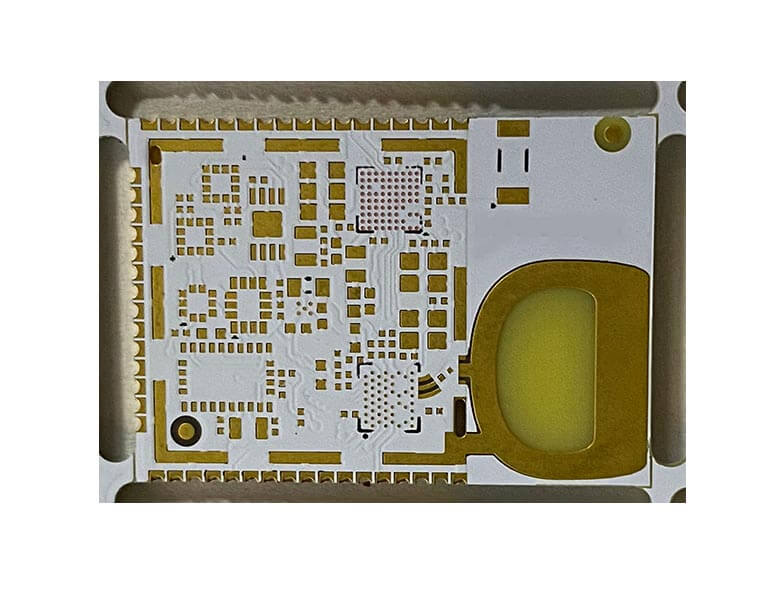
When hardware engineers ask, “What does High Density Interconnect mean in PCB?”, the answer lies in spatial efficiency. HDI (High Density Interconnect) is a PCB manufacturing technology that utilizes extremely fine lines, ultra-thin dielectric materials, and microscopic laser-drilled holes to pack a massive amount of circuitry into a fraction of the space required by a standard board.
To truly understand HDI, think of urban planning. A standard PCB is like a sprawling suburban neighborhood. Houses (components) are spread out, and wide roads (traces) take up a massive amount of surface area. When you run out of space, your only option is to build further outward, increasing the footprint.
HDI, on the other hand, is like building a skyscraper in downtown Manhattan. Because the footprint is strictly limited, you must build vertically. You use internal elevators (blind and buried vias) that do not take up space on every single floor, allowing you to house exponentially more functionality in a highly confined area.
For engineers who are transitioning from legacy designs to modern compact electronics, grasping this spatial shift is critical. If you are entirely new to this concept, you might want to review a comprehensive beginner’s guide to HDI PCBs to familiarize yourself with the foundational terminology before we dive into the complex engineering constraints.
Core Concepts Simplified
To successfully design an HDI board, you must understand the microscopic structures that make it possible. Let’s break down the complex terminology into plain English.
Microvias: The Laser Scalpel
In standard PCB manufacturing, vias are created using mechanical drill bits. Even the smallest mechanical drills (around 0.15mm to 0.20mm) are massive in the context of modern microelectronics, and they require even larger capture pads.
Microvias are holes typically 0.15mm (6 mils) or smaller in diameter. Instead of physical drill bits, manufacturers use high-energy precision lasers to ablate (burn away) the dielectric material. If a mechanical drill is a blunt construction hammer, a laser drill is a surgeon’s scalpel. It allows for incredibly tight tolerances and stops precisely at the target copper layer without penetrating further.
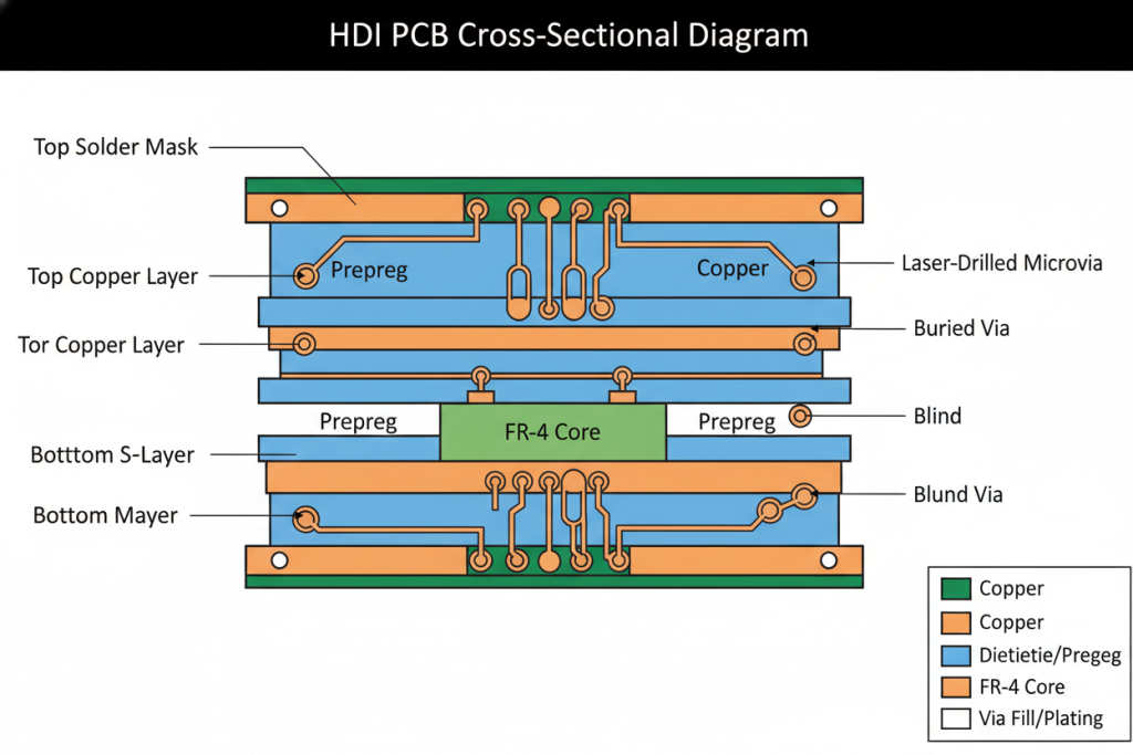
Blind and Buried Vias: The Secret Passages
Standard through-hole vias punch through every single layer of the board, from top to bottom. If you only need to connect Layer 1 to Layer 2, a through-hole via wastes valuable routing space on Layers 3 through 8.
- Blind Vias: These are like a private staircase leading from the ground floor (surface layer) down to a basement (internal layer), but no further. From the other side of the PCB, the hole is completely invisible (blind), leaving that surface area free for components.
- Buried Vias: Think of these as secret elevator shafts hidden entirely within the middle floors of a building. They connect internal layers (e.g., Layer 2 to Layer 3) but do not break the surface on either the top or bottom of the board.
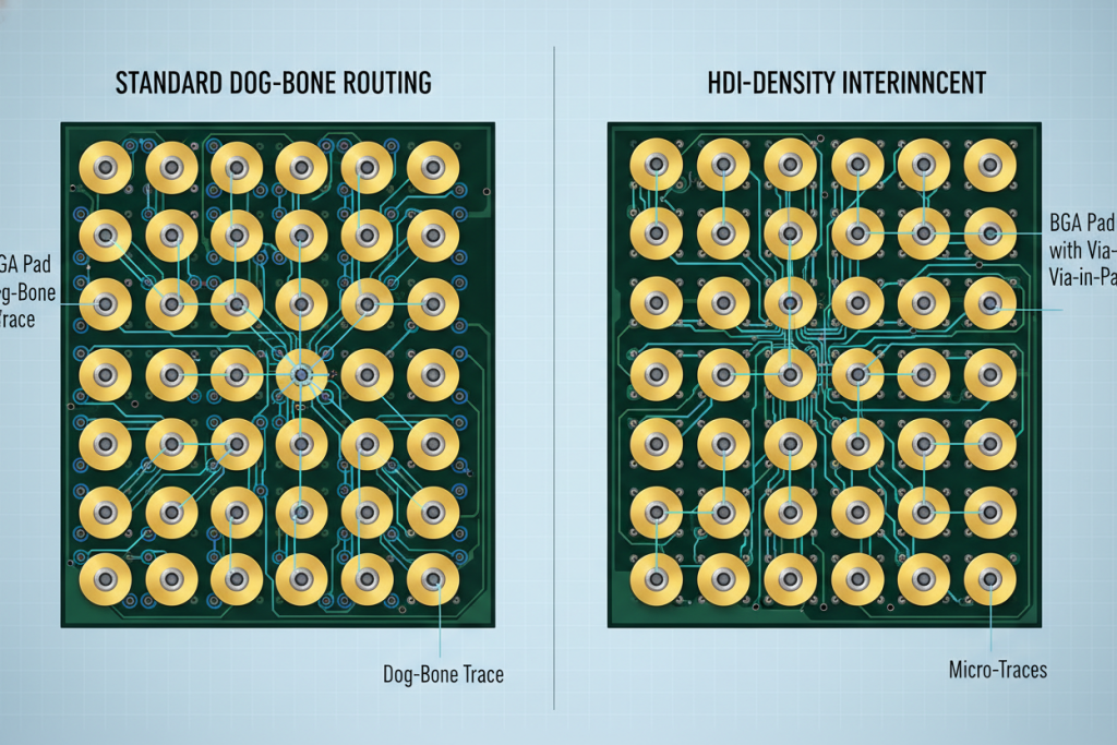
Via-in-Pad (VIPPO): The Ultimate Space Saver
When routing high pin-count Ball Grid Arrays (BGAs), traditional “dog-bone” fanouts (where a trace leads from the BGA pad to a via next to it) consume too much real estate.
Via-in-Pad technology places the microvia directly inside the component’s solder pad. To use a plumbing analogy: instead of drilling a drain hole in the floor next to your bathtub and running a pipe to it, Via-in-Pad puts the drain directly underneath the tub. The microvia is drilled, plated, filled with epoxy, and capped with copper so it remains perfectly flat for soldering. This is the ultimate “killer feature” for ultra-dense BGA routing.
Core Concept Comparison Table
| Technology | The Plain English Analogy | Technical Function & Benefit |
|---|---|---|
| Mechanical Via | Suburban sprawl | Large, physical drill hole. Wastes space on all layers. |
| Laser Microvia | Surgical scalpel | <0.15mm hole. Allows ultra-fine routing and smaller pads. |
| Blind Via | Basement staircase | Connects outer layer to inner layer. Saves space on opposite side. |
| Buried Via | Hidden elevator | Connects inner layers only. Frees up both outer surfaces. |
| Via-in-Pad | Drain under the bathtub | Via placed directly in solder pad. Mandatory for <0.5mm pitch BGAs. |
HDI PCB vs. Standard PCB: When to Make the Switch?
One of the most common debates on engineering forums like r/PrintedCircuitBoard is: “Do I really need to pay the premium for HDI on this project?”
Understanding the differences between HDI and standard PCBs is not just about knowing the specs; it is about recognizing the exact tipping point where standard routing mathematically fails or becomes economically unviable.
The Tipping Point: Scenario Analysis
You should not use HDI just because it sounds advanced. You switch to HDI when you hit specific physical constraints:
- Component Pitch Constraints: If your design includes a BGA with a pitch of 0.5mm or smaller, standard mechanical drilling cannot physically fit between the pads without violating the manufacturer’s annular ring tolerances. You must use HDI (specifically Via-in-Pad).
- Layer Count vs. Cost: Sometimes, reducing layer count justifies HDI. If a dense design requires a 12-layer standard PCB with complex routing, you might be able to condense it into an 8-layer HDI board (using a 2+4+2 stack-up). The savings in raw materials and lamination cycles can sometimes offset the higher cost of laser drilling.
- Signal Integrity Requirements: High-speed digital signals (like PCIe Gen 4/5 or high-speed DDR memory) suffer from “via stubs”—the unused portion of a through-hole via that acts as an antenna, causing signal reflections. Blind/buried microvias eliminate these stubs naturally, vastly improving signal integrity.
Why Modern Electronics Rely on HDI
If you look at the teardown of any modern flagship 5G smartphone, Apple Watch, or automotive ADAS radar module, you will find complex HDI boards (often using Any-Layer HDI technology).
The reasons they are predominantly used in modern electronics design go beyond just making things smaller. Shorter trace lengths mean faster signal transmission and lower power consumption. In battery-powered IoT devices and wearables, every millimeter of saved PCB space translates to a larger battery capacity, directly enhancing the user experience.
Specification Comparison: Standard vs. HDI
| Specification | Standard PCB | HDI PCB | Decision Trigger |
|---|---|---|---|
| Minimum Trace/Space | 4 mil / 4 mil | 2 mil / 2 mil (or less) | Need to route dense buses in tight spaces. |
| Smallest Via Hole Size | 0.15mm (Mechanical) | 0.075mm – 0.1mm (Laser) | BGA pitch < 0.5mm. |
| Via Pad Size | 0.35mm | 0.20mm – 0.25mm | High component density on surface. |
| Layer Stack-up | Symmetrical (e.g., 4, 6, 8) | Sequential (e.g., 1+N+1, 2+N+2) | Need for blind/buried vias to save space. |
| Signal Integrity | Prone to via stub reflections | Excellent (No via stubs) | High-speed RF, PCIe, or DDR5 routing. |
Expert Tips & Common Pitfalls to Avoid in HDI Design
Transitioning to HDI introduces strict manufacturing constraints. Based on real-world failures and feedback from hardware engineering communities, here are the most critical pitfalls to avoid to ensure high manufacturing yield.
Pitfall 1: Ignoring the Microvia Aspect Ratio
The aspect ratio is the ratio of the dielectric thickness to the microvia hole diameter. Because microvias are tiny, it is difficult for manufacturers to plate copper deep inside them.
- The Rule: Keep your microvia aspect ratio at 0.75:1 (ideal) or 1:1 (absolute maximum). For example, if your laser drill hole is 4 mils (0.1mm), the dielectric layer it penetrates must not be thicker than 4 mils. If you ignore this, the copper plating will fail, resulting in a dead board.
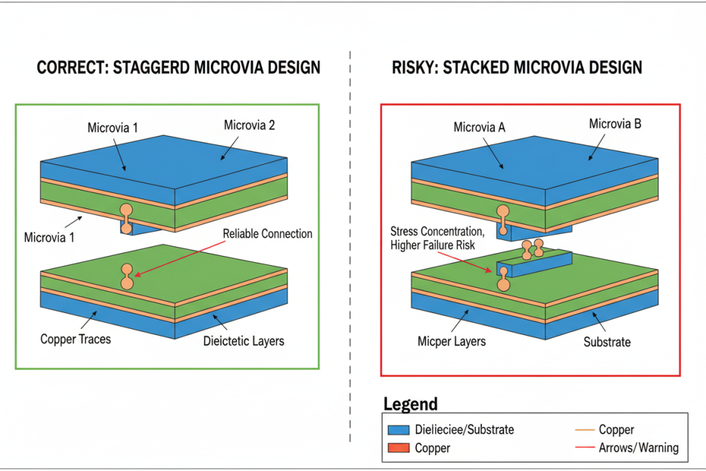
Pitfall 2: Stacked vs. Staggered Vias
When you need to drop down multiple layers (e.g., Layer 1 to Layer 3), you have two choices:
- Stacked Vias: Placing a microvia directly on top of another microvia. While this saves the most space, it is incredibly difficult to manufacture. It requires the bottom via to be perfectly filled and planarized. Tiny trapped air bubbles can cause the via to explode during reflow soldering.
- Staggered Vias: Offsetting the microvias slightly like a staircase.
- Expert Tip: Always default to staggered vias unless your space constraints absolutely force you to use stacked vias. Staggered vias are cheaper, have higher yields, and are much more reliable.
Pitfall 3: Poor Via-in-Pad Capping
If you use Via-in-Pad without specifying proper filling and capping, the solder paste will wick down into the hole during assembly. This starves the BGA pad of solder, leading to open circuits or weak mechanical bonds.
- The Fix: Always specify POFV (Plated Over Filled Via) or IPC-4761 Type VII in your fabrication notes. The manufacturer must fill the via with epoxy and plate copper over it so it is completely flush.
Conclusion & Final Thoughts
High Density Interconnect (HDI) is no longer a niche technology reserved for aerospace or flagship smartphones; it is the standard for modern, compact, high-performance electronics. By replacing bulky mechanical drills with precision laser microvias, and utilizing blind/buried vias alongside via-in-pad technology, engineers can achieve routing densities that were impossible a decade ago.
However, HDI is not a silver bullet. It requires a fundamental shift in how you approach PCB layout, stack-up design, and manufacturing constraints like aspect ratios and via staggering.
Quick Summary Table: HDI Decision Matrix
| Factor | Standard PCB | HDI PCB |
|---|---|---|
| Best For | Prototyping, large form factors, low-speed signals. | Wearables, IoT, smartphones, high-speed digital. |
| Cost | Lower initial fabrication cost. | Higher fab cost, but can reduce overall layer count. |
| Design Complexity | Low to Medium. Standard DRC rules apply. | High. Requires careful stack-up planning (1+N+1, etc.). |
| Key Enabler | Mechanical drilling. | Laser microvias & Via-in-Pad. |
Before you route your next compact device, evaluate your component pitches and routing density. If you are crossing the threshold into sub-0.5mm BGAs or struggling to maintain signal integrity on high-speed traces, it is time to upgrade your design methodology.
To ensure your HDI designs transition smoothly from CAD to physical reality without costly yield issues, partnering with an experienced manufacturer is crucial. Explore options for reliable HDI PCB manufacturing to get expert stack-up advice and DFM (Design for Manufacturing) checks before you finalize your Gerber files.