As electronics shrink and performance demands skyrocket, hardware engineers are hitting a physical wall. You have a massive BGA component, hundreds of pins, and a board footprint that is continually shrinking. The critical dilemma arises: do you stick with a reliable, cost-effective 2-layer HDI (2+N+2) structure, or is it time to bite the bullet and invest in a 3-layer HDI (3+N+3) architecture?
Making the wrong choice here doesn’t just mean a failed prototype; it means catastrophic yield drops, budget overruns, and delayed time-to-market. In this guide, we will dissect the exact technical and financial “Tipping Points” between 2-layer and 3-layer HDI. You will learn how to evaluate BGA pitch, manufacturing tolerances, and signal integrity to make a data-driven decision for your next high-density project.
In the high-tech sectors of telecommunications, medical devices, and aerospace, standard printed circuit boards (PCBs) simply cannot handle the routing density required by modern silicon. High-Density Interconnect (HDI) technology solves this by utilizing laser-drilled microvias, finer lines, and thinner materials to pack more functionality into a smaller space.
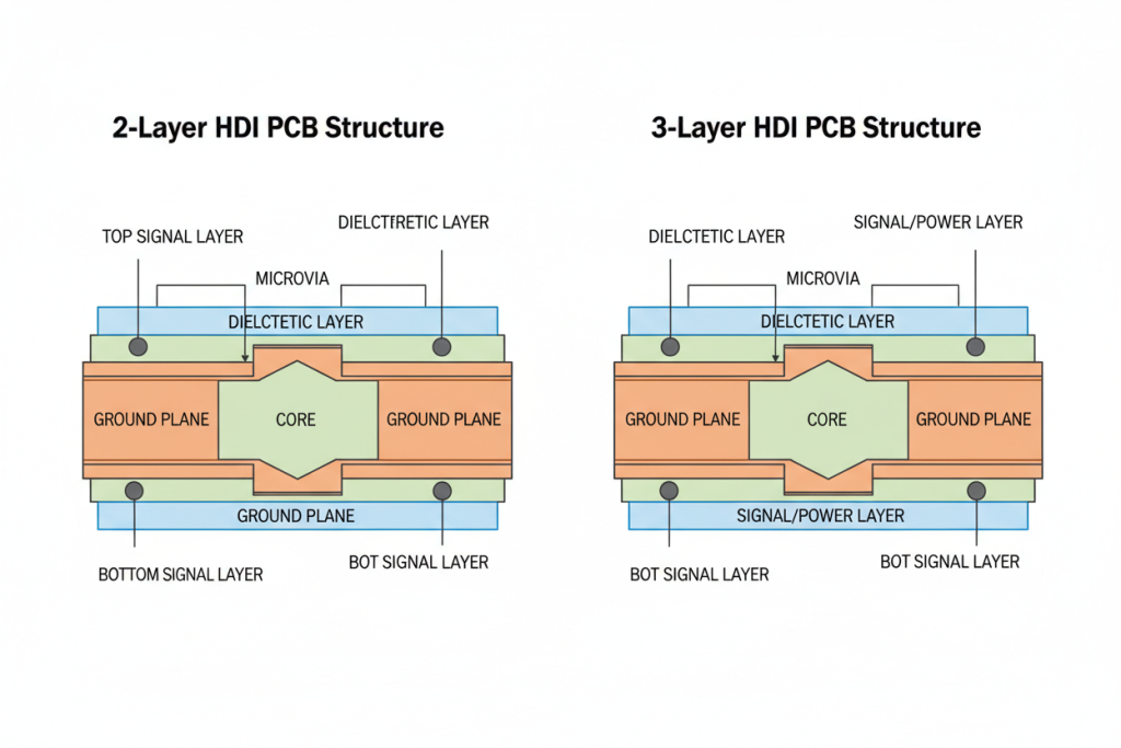
However, scaling your design from standard PCBs to HDI is not a linear journey. The industry standardizes HDI structures using an “X+N+X” nomenclature.
“N” represents the standard, mechanically drilled core layers.
“X” represents the number of sequential HDI build-up layers added to each side of the core.
A 2-Layer HDI (2+N+2) means there are two layers of high-density laser microvias on top and bottom. A 3-Layer HDI (3+N+3) adds a third layer of extreme density.
The leap from 2 to 3 layers is not just an incremental step; it is a fundamental shift in manufacturing complexity, thermal stress, and cost. Partnering with a facility capable of high-quality pcb manufacturing becomes non-negotiable at this stage, as the margin for error shrinks to microscopic levels.
Core Concepts Simplified
To make an informed decision, we must translate complex manufacturing jargon into plain English. Let’s break down the core mechanics of HDI using a simple analogy.
Imagine your PCB is a high-rise office building, and the electrical signals are office workers trying to get from the roof to the lobby.
Through-Hole Vias: The traditional, slow staircase that goes from the top floor all the way to the bottom. It takes up a massive amount of floor space on every single level.
Microvias: High-speed express elevators that only travel between one or two specific floors. They save immense amounts of floor space (routing area) but require complex engineering to install.
The “N+2” vs “N+3” Structural Shift
Using the elevator analogy, a 2-layer HDI provides two sets of express elevators to connect the outer floors. It is highly efficient for most modern traffic. A 3-layer HDI adds a third, incredibly complex elevator system designed exclusively for ultra-high-speed data and extreme population density.
Microvia Aspect Ratio
This is the ratio of the laser-drilled hole’s depth to its width. If a microvia is too deep and too narrow, the copper plating process will fail to fill it completely. Think of trying to paint the inside of a long, thin straw. If the copper doesn’t fill the via correctly, the connection will break under thermal stress.
Sequential Laminations
This is the process of pressing the PCB layers together using extreme heat and pressure. A 2-layer HDI requires the board to be pressed twice. A 3-layer HDI requires three separate presses. Every time the board goes into the press, it is subjected to thermal shock, which can warp the materials and misalign the microscopic copper pads.
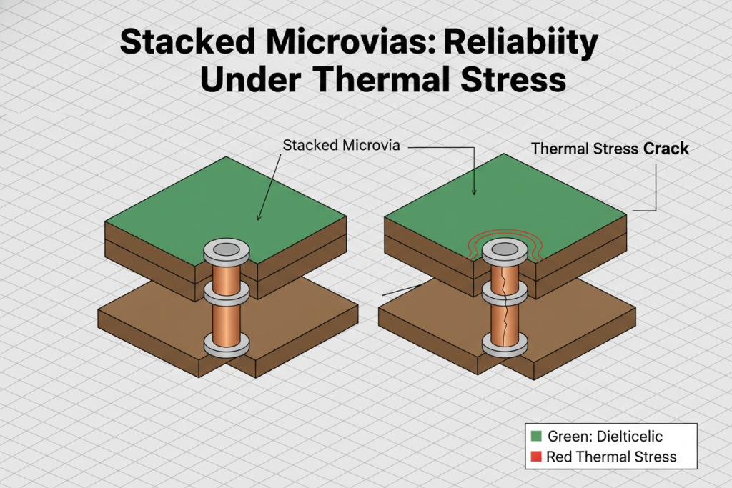
Staggered vs. Stacked Vias
Staggered Vias: Like a staircase, the microvias are offset from one another. They are easier to manufacture and highly reliable.
Stacked Vias: Like a direct ladder, microvias are placed directly on top of each other. They save the maximum amount of space but are notoriously difficult to manufacture reliably, as any misalignment causes the entire “tower” to fail.
Core Concept Comparison Table
Feature
2-Layer HDI (2+N+2)
3-Layer HDI (3+N+3)
Sequential Laminations
2 Presses (Moderate thermal stress)
3 Presses (High thermal stress)
Manufacturing Cost
Baseline HDI Cost ($$)
Premium Cost (1.5x to 2x higher) ($$$$)
Yield Rate
High (Typically 90%+)
Lower (Highly dependent on factory capability)
Routing Density
High (Suitable for most smartphones/IoT)
Extreme (Required for dense FPGAs/Telecom)
Via Structure
Mostly Staggered, some Stacked
Heavy use of Stacked Vias across 3 layers
Step-by-Step Guide: Choosing Your Stackup
The decision between 2-layer and 3-layer HDI almost always comes down to one critical metric: BGA Pitch.
The “Parking Lot” Analogy: Think of the pins on the bottom of your BGA (Ball Grid Array) chip as cars in a parking lot. The “Pitch” is the distance between these cars. If the cars are parked comfortably apart (0.65mm or 0.5mm pitch), you have enough room to build roads (copper traces) to drive them out. However, if the cars are crammed tightly together (0.4mm pitch or lower), there is no room for roads on the surface. You must build underground tunnels (microvias) to drop the traffic down to lower levels before routing them out. The tighter the cars are packed, the deeper and more complex the tunnels need to be.
Scenario A: When 2-Layer HDI is the Perfect Fit
You should default to a 2+N+2 structure whenever physically possible to maximize your Return on Investment (ROI) and manufacturing yield.
Ideal Parameters for 2-Layer HDI:
BGA Pitch: 0.5mm or larger.
Pin Count: Under 400 pins.
Application: Consumer electronics, standard automotive modules, and mid-tier medical devices.
In this scenario, you can easily use staggered microvias to escape the BGA footprint. The manufacturing process is stable across most global fabricators, ensuring a highly competitive cost-per-board.
Scenario B: The Tipping Point for 3-Layer HDI
Upgrading to 3+N+3 should be a forced decision, driven by mathematical constraints rather than a desire to “over-engineer.”
You MUST upgrade to 3-Layer HDI when:
BGA Pitch: 0.4mm or smaller.
Pin Count: 500+ pins (especially large FPGAs or network switches).
Signal Integrity: You are routing 10Gbps+ signals and need absolute control over parasitic capacitance, which requires extremely short, stacked microvias.
When you enter this territory, the tolerances become unforgiving. Similar to the extreme precision required in 50-layer pcb manufacturing, a 3-layer HDI board demands perfect registration between layers. If the laser drill misses the target pad by even a few microns on the third lamination cycle, the entire board is scrapped.
Technical Specification Matrix for Stackup Selection
Design Constraint
Go with 2-Layer HDI (2+N+2)
Upgrade to 3-Layer HDI (3+N+3)
Minimum BGA Pitch
$\ge$ 0.5mm
$\le$ 0.4mm
I/O Pin Count
< 500 Pins
> 500 Pins
High-Speed Signals
Up to 10 Gbps (Manageable)
10 Gbps to 25+ Gbps (Optimal)
Via Architecture
Staggered Vias sufficient
Stacked Vias (L1-L4) mandatory
Board Thickness
Standard (1.0mm – 1.6mm)
Often requires thinner dielectrics
🛠️ AI Prompt Template: HDI Stackup Selection
If you are unsure where your design falls, you can use this prompt in any AI assistant (like ChatGPT or Claude) to get a baseline recommendation before consulting your manufacturer.
Expert Tips & Common Pitfalls to Avoid
When browsing engineering subreddits or hardware forums, you will frequently see horror stories of HDI projects failing during the prototype phase. Here are the most common pitfalls and how to avoid them based on real-world manufacturing experience.
Pitfall 1: Overusing Stacked Vias
The Mistake: Designers often stack microvias across 3 or 4 layers because it looks clean and saves space in the CAD software. The Reality: Stacked vias are the “Achilles’ heel” of HDI reliability. Every time you stack a via, you increase the risk of plating voids and thermal expansion failures. The Fix: Always prefer staggered vias. Only use stacked vias when the BGA pitch physically forces you to.
Pitfall 2: Ignoring Thermal Stress from Sequential Laminations
The Mistake: Assuming the FR4 material will behave the same on the third lamination cycle as it did on the first. The Reality: Repeated exposure to the lamination press degrades the resin and causes the board to expand and contract. Just as you must carefully manage material stability in rigid-flex pcb design guidelines, you must choose high-Tg (Glass Transition Temperature) materials for 3-layer HDI to survive the triple-press process.
Pitfall 3: Failing to Verify the Aspect Ratio
The Mistake: Designing a microvia that is 5 mils wide but needs to go through an 8-mil thick dielectric layer. The Reality: The aspect ratio exceeds 1:1. The manufacturer’s plating chemicals cannot circulate at the bottom of that hole, leaving it hollow. When the board heats up, the thin copper will crack. The Fix: Keep your microvia aspect ratio strictly at or below 0.8:1 (Depth:Width).
Conclusion & Final Thoughts
Choosing between a 2-layer and 3-layer HDI PCB is not a matter of preference; it is a strict mathematical calculation based on your component density, signal integrity needs, and budget tolerance.
The “Tipping Point” is clear: If your BGA pitch drops to 0.4mm or below, and your pin counts exceed 500, the 3+N+3 architecture transitions from an expensive luxury to an absolute engineering necessity. However, if you can comfortably route your signals with a 0.5mm pitch, sticking to a 2+N+2 structure will drastically improve your manufacturing yields, reduce lead times, and protect your profit margins.
Frequently Asked Questions (FAQ)
Q1: What is the difference between 2-layer HDI (2+N+2) and 3-layer HDI (3+N+3)? A: 2-layer HDI has two sequential build-up layers of laser microvias on each side of the core, requiring 2 lamination presses. 3-layer HDI adds a third build-up layer, requiring 3 presses and enabling extreme routing density for 0.4mm pitch BGAs and 500+ pin counts.
Q2: When should I upgrade from 2-layer to 3-layer HDI? A: Upgrade to 3-layer HDI when your BGA pitch drops to 0.4mm or smaller, your pin count exceeds 500, or you are routing 10Gbps+ signals requiring stacked microvias for parasitic capacitance control. For 0.5mm+ pitch and under 400 pins, 2-layer HDI is sufficient.
Q3: What is the maximum recommended microvia aspect ratio? A: Keep the microvia aspect ratio (depth:width) at or below 0.8:1. Exceeding 1:1 causes plating chemicals to fail at the via bottom, leaving hollow vias that crack under thermal stress.
Q4: Should I use staggered or stacked vias in HDI design? A: Always prefer staggered vias—they are more reliable and easier to manufacture. Only use stacked vias when BGA pitch constraints (0.4mm or below) physically force you to, as they carry higher plating void and thermal expansion risks.
Q5: How does sequential lamination affect HDI manufacturing yield? A: Each lamination press subjects the board to thermal shock that can warp materials and misalign pads. 2-layer HDI survives 2 presses with 90%+ yield. 3-layer HDI requires 3 presses with high-Tg materials and top-tier fabricators to maintain acceptable yield rates.
Q6: What BGA pitch requires 3-layer HDI architecture? A: BGA pitches of 0.4mm or smaller typically require 3-layer HDI because there is insufficient surface area between pads for standard trace routing. At 0.5mm or larger, 2-layer HDI with staggered microvias can usually escape the BGA footprint.
Cookie Consent
We use cookies to improve your experience on our site. By using our site, you consent to cookies.
Used to monitor number of Google Analytics server requests when using Google Tag Manager
1 minute
_ga_
ID used to identify users
2 years
_gid
ID used to identify users for 24 hours after last activity
24 hours
_gali
Used by Google Analytics to determine which links on a page are being clicked
30 seconds
_ga
ID used to identify users
2 years
__utmx
Used to determine whether a user is included in an A / B or Multivariate test.
18 months
__utmv
Contains custom information set by the web developer via the _setCustomVar method in Google Analytics. This cookie is updated every time new data is sent to the Google Analytics server.
2 years after last activity
__utmz
Contains information about the traffic source or campaign that directed user to the website. The cookie is set when the GA.js javascript is loaded and updated when data is sent to the Google Anaytics server
6 months after last activity
__utmc
Used only with old Urchin versions of Google Analytics and not with GA.js. Was used to distinguish between new sessions and visits at the end of a session.
End of session (browser)
_gac_
Contains information related to marketing campaigns of the user. These are shared with Google AdWords / Google Ads when the Google Ads and Google Analytics accounts are linked together.
90 days
__utmb
Used to distinguish new sessions and visits. This cookie is set when the GA.js javascript library is loaded and there is no existing __utmb cookie. The cookie is updated every time data is sent to the Google Analytics server.
30 minutes after last activity
__utmt
Used to monitor number of Google Analytics server requests
10 minutes
__utma
ID used to identify users and sessions
2 years after last activity
SourceBuster is used by WooCommerce for order attribution based on user source.
Name
Description
Duration
sbjs_migrations
Technical data to help with migrations between different versions of the tracking feature
session
sbjs_current_add
Timestamp, referring URL, and entry page for your visitor’s current visit to your store
session
sbjs_first_add
Timestamp, referring URL, and entry page for your visitor’s first visit to your store (only applicable if the visitor returns before the session expires)
session
sbjs_current
Traffic origin information for the visitor’s current visit to your store
session
sbjs_first
Traffic origin information for the visitor’s first visit to your store (only applicable if the visitor returns before the session expires)
session
sbjs_udata
Information about the visitor’s user agent, such as IP, the browser, and the device type
session
sbjs_session
The number of page views in this session and the current page path