Metal Core PCB Stack Up Explained: 1-Layer to Multi-Layer Configurations
When designing high-power electronics, thermal management becomes critical. Metal Core PCBs (MCPCBs) offer a specialized stack-up architecture that channels heat away from components more effectively than traditional FR-4 boards. This guide breaks down MCPCB layer configurations from single-layer to complex multi-layer designs, helping you choose the right stack-up for your thermal requirements.
What is Metal Core PCB Stack-Up?
Metal Core PCB stack-up refers to the layered structure that combines conductive copper circuits with a thermally conductive metal substrate. Unlike standard PCBs that use fiberglass (FR-4) as the base material, MCPCBs replace this with aluminum or copper to create a direct thermal path from heat-generating components to external cooling systems.
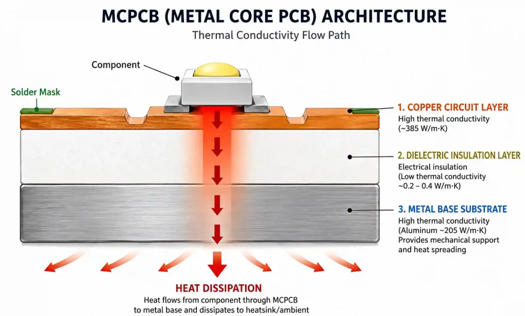
The fundamental MCPCB stack consists of three essential layers:
- Copper circuit layer – Contains your circuit traces and component pads
- Dielectric insulation layer – Provides electrical isolation while maintaining thermal conductivity
- Metal base substrate – Acts as both structural support and heat spreader
This architecture transfers heat 8-10 times faster than traditional FR-4 boards, making MCPCBs indispensable for LED lighting, power converters, automotive electronics, and industrial motor drives where thermal performance directly impacts reliability and lifespan.
Single-Layer MCPCB Configuration
Single-layer MCPCBs dominate the market, representing approximately 90% of all metal core board applications. This configuration places all circuit traces on one side of the board, directly above the metal substrate.
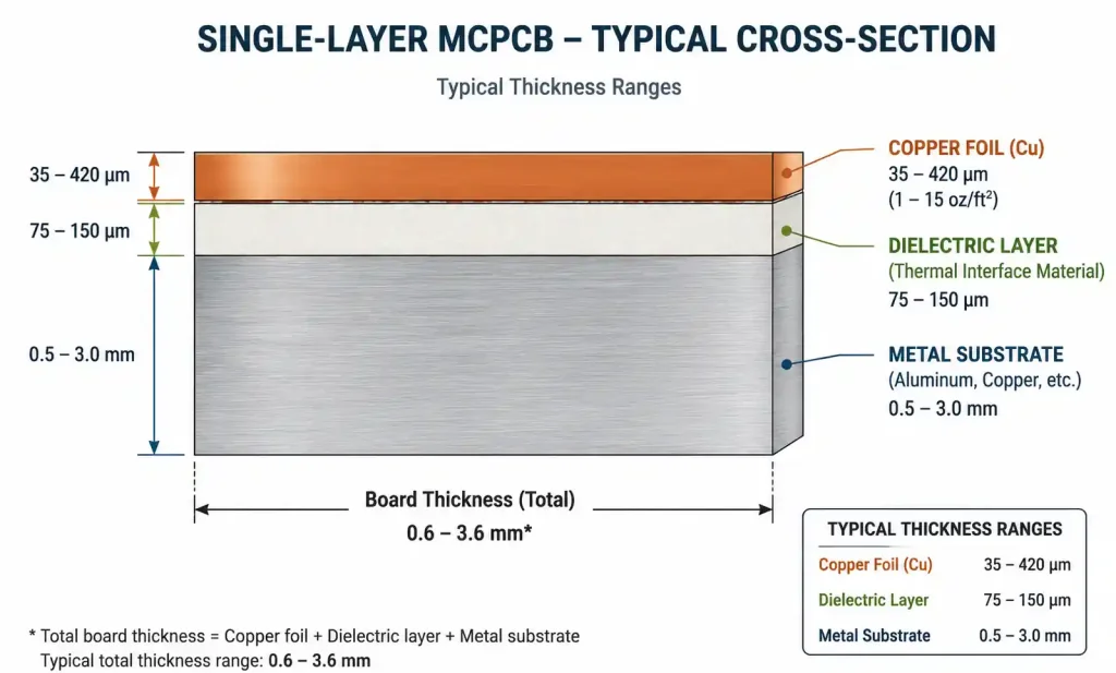
Typical single-layer stack-up structure:
- Top copper foil: 35μm to 420μm (1-12 oz)
- Dielectric layer: 75μm to 150μm
- Metal substrate: 0.5mm to 3.0mm (typically 1.0-1.6mm)
Key design constraint: The dielectric layer cannot be drilled through, eliminating the possibility of plated through-holes (PTH). All connections must remain on the top surface, which simplifies manufacturing but limits routing flexibility.
Advantages:
- Lower cost compared to multi-layer designs
- Excellent thermal performance for straightforward layouts
- Easier manufacturing and shorter lead times
- Ideal for LED arrays and simple power circuits
Limitations:
- No component placement on bottom side
- Limited routing options without PTH
- Single ground plane reference
Double-Layer Metal Core Stack-Up
Double-layer aluminum PCBs introduce a second copper circuit layer, connected through plated through-holes. This configuration dramatically expands routing possibilities while maintaining strong thermal performance.
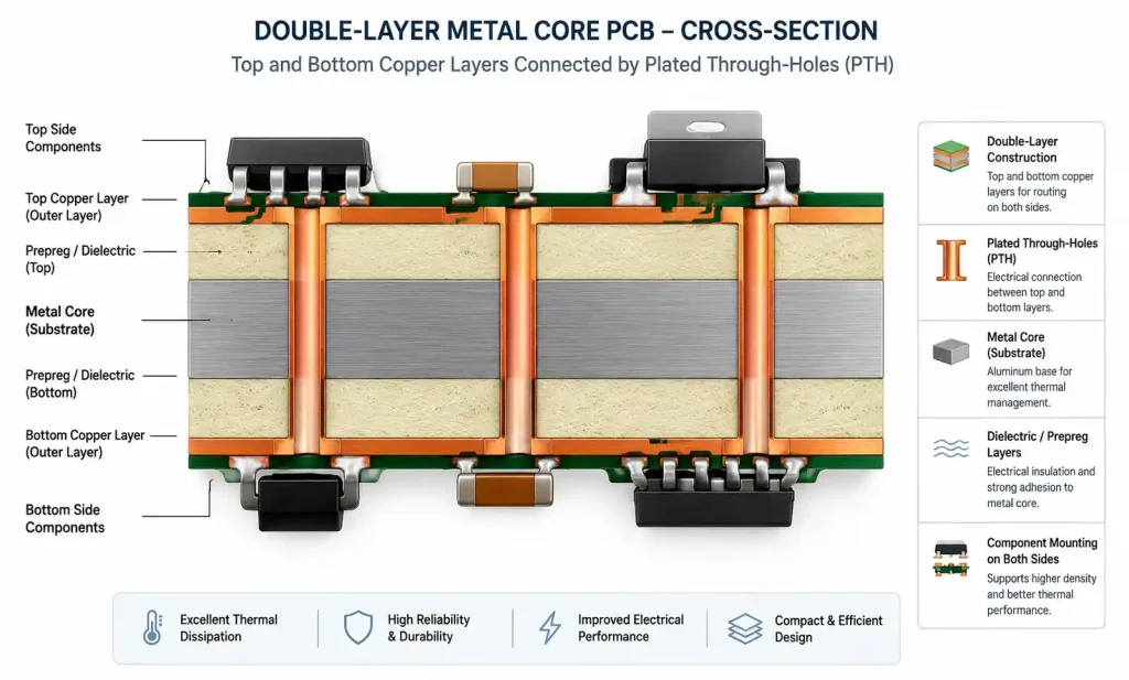
Typical double-layer structure:
- Top copper layer: 35μm to 105μm
- Dielectric/prepreg: 100μm to 200μm
- Bottom copper layer: 35μm to 105μm
- Dielectric insulation: 75μm to 150μm
- Metal substrate: 1.0mm to 2.0mm
Thermal conductivity: Maintains 1-3 W/mK through the metal core despite the additional layers.
Design flexibility improvements:
- Component mounting on both sides
- Through-hole connections between layers
- Ground planes on separate layers
- Better signal integrity through layer separation
Trade-offs:
- Higher manufacturing cost
- More complex thermal modeling required
- Potential for thermal vias to impact heat flow
- Thicker overall board profile
Multi-Layer MCPCB Architecture
Multi-layer metal core boards (4+ layers) represent the premium segment, combining complex circuit routing with advanced thermal management. These designs integrate control circuits with high-power sections in a single board.
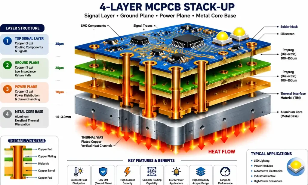
Common 4-layer hybrid structure:
- Layer 1 (Top): Signal/component layer
- Layer 2: Ground plane
- Layer 3: Power plane
- Dielectric insulation: Thermal interface
- Metal core: Aluminum or copper base
Advanced configurations may feature thermal vias strategically placed to create vertical heat channels, connecting hot components on upper layers directly to the metal core.
When to use multi-layer MCPCB:
- Complex mixed-signal designs requiring multiple ground planes
- High-density power supplies with digital control circuits
- Automotive systems combining sensors and power electronics
- Industrial equipment with integrated motor drives
Design complexity:
Balancing signal integrity, EMI control, and thermal pathways becomes critical. The metal core typically connects to system ground, providing excellent EMC shielding while serving as the primary heat spreader.
Layer Materials and Thickness Specifications
Material selection directly impacts thermal performance, electrical isolation, and mechanical reliability. Understanding the properties of each layer helps optimize your stack-up.
Copper Circuit Layer Options:
| Copper Weight | Thickness | Typical Use |
|---|---|---|
| 1 oz | 35μm | Standard signal circuits |
| 2 oz | 70μm | Moderate current applications |
| 3 oz | 105μm | Power distribution |
| 4-12 oz | 140-420μm | High-current power electronics |
Dielectric Materials:
- Standard epoxy: 1-2 W/mK thermal conductivity
- Ceramic-filled: 2-4 W/mK (improved thermal transfer)
- Aluminum oxide: 20-30 W/mK (premium applications)
Metal Substrate Choices:
- Aluminum 5052: Most common, excellent thermal conductivity (138 W/mK), lightweight
- Aluminum 6061: Higher strength, good machinability
- Copper: Superior thermal performance (385 W/mK) but heavier and more expensive
- Stainless steel: Special applications requiring rigidity
Thickness impact on thermal resistance:
A thicker metal substrate (3mm vs 1mm) reduces the board’s thermal resistance by approximately 40-50%, but increases weight and cost. For most LED and power applications, 1.5-2.0mm provides the optimal balance.
Thermal Management Through Stack Design
The stack-up architecture defines the thermal resistance path from component junction to ambient environment. Proper layer configuration ensures heat flows efficiently through the intended pathway.
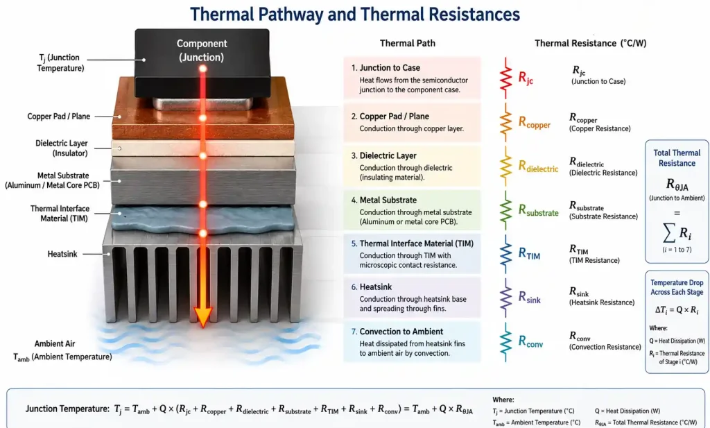
Thermal resistance chain:
- Component to copper pad (R_jc): Junction-to-case resistance
- Copper trace spreading (R_copper): Lateral heat distribution
- Dielectric interface (R_dielectric): Critical bottleneck in thermal path
- Metal substrate conduction (R_metal): Heat spreading to mounting interface
- Substrate to heatsink (R_interface): Thermal interface material matters
- Heatsink to ambient (R_sa): Final heat rejection
Design strategies for optimal thermal performance:
Position high-power components strategically: Place heat-generating devices directly over mounting holes or areas with good thermal coupling to external heatsinks. Centering power LEDs or MOSFETs along the primary heat dissipation axis reduces thermal resistance by 20-35%.
Maximize copper pad area: Larger copper pads act as heat spreaders before thermal energy crosses the dielectric interface. Expanding pad size by 50% can reduce local junction temperatures by 5-10°C.
Minimize dielectric thickness: The dielectric layer typically contributes 60-80% of total thermal resistance in the stack-up. Using 75μm instead of 150μm dielectric can cut thermal resistance nearly in half.
Use thermal vias in multi-layer designs: Copper-filled vias create vertical thermal highways, allowing heat to bypass insulating layers and reach the metal core directly.
Performance target: Properly designed MCPCB stack-ups should achieve ≤45°C temperature rise at 1W power dissipation, representing a 40%+ thermal efficiency improvement over FR-4.
Design Constraints and Best Practices
Metal Core PCB stack-up design involves unique constraints that differ from standard PCB fabrication. Understanding these limitations prevents costly redesigns.
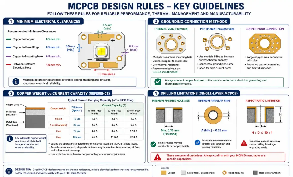
Critical design rules:
No drilling through dielectric in single-layer boards: Since the dielectric cannot be penetrated, all connections must route on the top surface. This eliminates traditional through-hole components in the thermal zone—use surface-mount devices exclusively.
Metal core grounding requirements: The metal substrate typically connects to system ground or remains floating for high-voltage isolation. If grounded, ensure proper connection through mounting hardware or dedicated grounding points.
Minimum clearances for high voltage:
- 0.5mm clearance for standard applications
- 1.0mm+ for high-voltage isolation (>150V)
- Extended creepage distances as voltage increases
Copper weight selection: Heavier copper (3-4 oz) improves current capacity and thermal spreading but increases manufacturing cost and makes fine-pitch routing difficult. Match copper weight to current requirements:
- ≤2A per trace: 1-2 oz copper
- 2-5A per trace: 2-3 oz copper
- >5A per trace: 4+ oz copper
Panelization considerations: MCPCBs require v-scoring or routing for separation—tab routing is standard since the metal substrate cannot be easily snapped like FR-4.
Testing and inspection: X-ray inspection may be necessary for complex assemblies since visual inspection cannot verify the dielectric/metal interface integrity.
Aluminum vs Copper Core Comparison
Choosing between aluminum and copper substrates significantly impacts thermal performance, weight, and cost. Each material suits different application requirements.
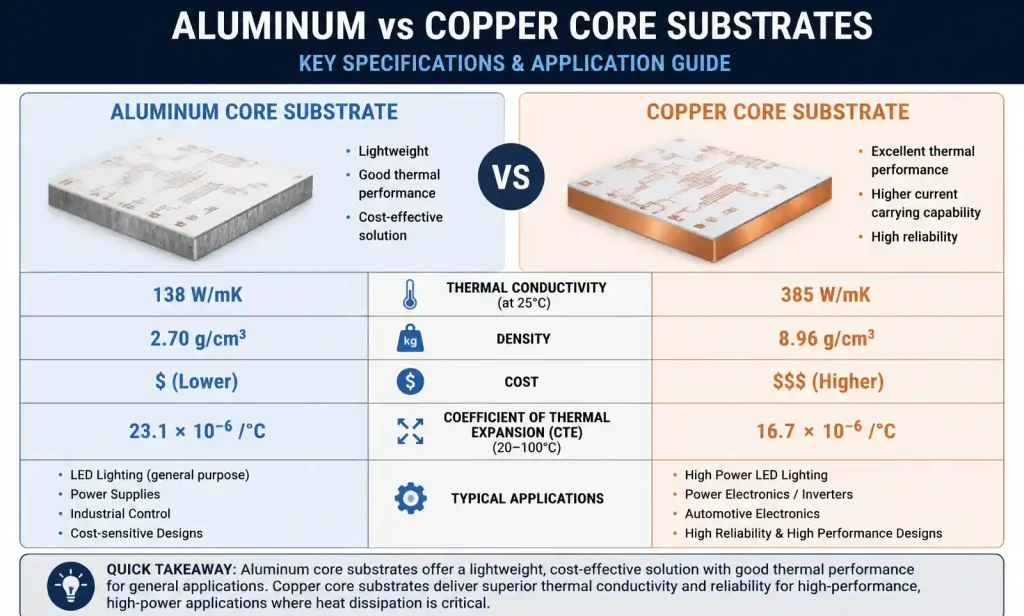
Aluminum Core Advantages:
- Cost-effective: 3-5x less expensive than copper
- Lightweight: Density of 2.7 g/cm³ vs copper’s 8.9 g/cm³
- Adequate thermal conductivity: 138 W/mK handles most applications
- Easier machining: Softer material simplifies routing and drilling
- Non-magnetic: Critical for RF and sensitive measurement equipment
Copper Core Advantages:
- Superior thermal performance: 385 W/mK—nearly 3x better than aluminum
- CTE matching: Copper’s thermal expansion (17 ppm/°C) closely matches FR-4 and ceramic components, reducing mechanical stress
- Higher current capacity: Better electrical conductivity for power distribution
- Extreme temperature applications: Maintains properties at higher operating temperatures
Hybrid approaches: Some advanced designs use copper cores in high-heat zones (under power semiconductors) with aluminum in lower-stress areas to balance performance and cost.
Selection guidelines:
- LED lighting, general electronics: Aluminum (cost-effective, sufficient performance)
- High-power RF amplifiers: Copper (superior heat spreading)
- Automotive under-hood: Copper (temperature cycling resilience)
- Consumer electronics: Aluminum (weight and cost priority)
Applications by Stack Configuration
Different stack-up configurations serve specific application requirements. Matching your thermal demands to the appropriate MCPCB structure ensures optimal performance and cost-effectiveness.
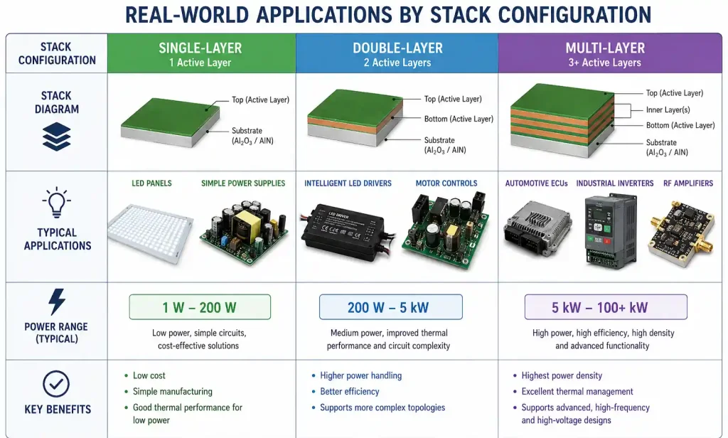
Single-Layer Applications:
- LED lighting panels: Street lights, architectural lighting, horticultural grow lights
- Simple power supplies: AC-DC converters, linear regulators
- Automotive lighting: Headlights, taillights, interior lighting
- Typical power range: 1-50W per board
Double-Layer Applications:
- Intelligent LED drivers: Dimming control, color tuning circuits
- Motor control modules: Gate drivers, current sensing, control logic
- Power management ICs: Buck/boost converters with digital control
- Typical power range: 20-200W per board
Multi-Layer Applications:
- Automotive ECUs: Engine control units combining power outputs and microcontroller circuits
- Industrial inverters: Three-phase motor drives with integrated control
- RF power amplifiers: Base station equipment, radar systems
- Medical equipment: Surgical lighting, diagnostic imaging power systems
- Typical power range: 100W-1kW+ per board
Emerging applications include electric vehicle battery management systems (BMS), wireless charging pads, and 5G telecommunications infrastructure—all demanding sophisticated thermal management through optimized stack-up design.
Conclusion
Metal Core PCB stack-up design fundamentally reshapes how we approach thermal management in electronics. From single-layer LED boards to complex multi-layer power systems, the strategic arrangement of copper, dielectric, and metal substrate determines whether your design operates reliably or fails prematurely due to thermal stress.
The key takeaways: single-layer configurations handle 90% of applications cost-effectively; double-layer designs add routing flexibility when needed; multi-layer structures tackle the most demanding thermal challenges. Material selection—aluminum versus copper, dielectric thickness, copper weight—directly impacts thermal resistance and should align with your power dissipation requirements.
As power densities continue increasing across LED, automotive, and industrial electronics, mastering MCPCB stack-up principles becomes essential. The 8-10x thermal improvement over FR-4 isn’t just a specification—it’s the difference between a product that thrives in the field and one that fails within warranty.